Semiconductor device module

a technology of semiconductor devices and modules, applied in the field of semiconductor devices, can solve the problems of insufficient carrying capacity, inability to find and find ranges, and impaired reliability of range finder modules, and achieve the effect of wide bonding area and higher adhesion strength

Inactive Publication Date: 2005-06-14
FUJI ELECTRIC CO LTD
View PDF11 Cites 68 Cited by
  • Summary
  • Abstract
  • Description
  • Claims
  • Application Information

AI Technical Summary

Benefits of technology

[0014]When an adhesive is coated on the U-groove including a pedestal disposed on the central bottom portion of the U-groove and a sensor chip is pressed onto a predetermined location on the pedestal, the adhesive expands to the space surrounding the pedestal and fills the space between the back surface of the sensor chip and the bottom of the U-groove. Since the spaces having no steps are left between the side walls of the U-groove and the pedestal, the adhesive provided with a way to escape does not splash to the outside. Therefore, the voids, which pose problems to the related semiconductor device module, are prevented from causing and a wide bonding area is obtained between the sensor chip and the sensor stage.
[0015]The adhesive is preferably a thermosetting and UV-curing adhesive. By employing primary UV-curing and secondary thermosetting, a higher adhesion strength is obtained.

Problems solved by technology

The assembly process of mounting a sensor chip on the sensor stage having the related structure described above poses several problems.
Furthermore, it has been observed that the adhesive sticking to the central portion on the back surface of the sensor chip 4 is cured insufficiently, since the ultraviolet ray irradiated downward onto the sensor stage 3 in the UV-curing step does not well reach the central portion on the back surface of the sensor chip 4, causing carriers of an insufficient amount.
Once the adhesion defects as described above are caused in the manufacturing process, the sensor chip 4 will part unexpectedly from the sensor chip 3 by the impact exerted to the range finder module, causing incapability of range finding and such troubles.
Thus, the reliability of the range finder module is impaired.

Method used


Image

  • Semiconductor device module
  • Semiconductor device module
  • Semiconductor device module

Examples


Embodiment Construction

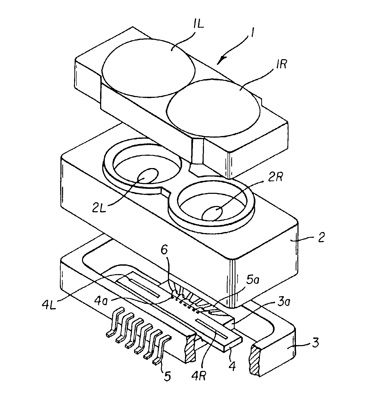
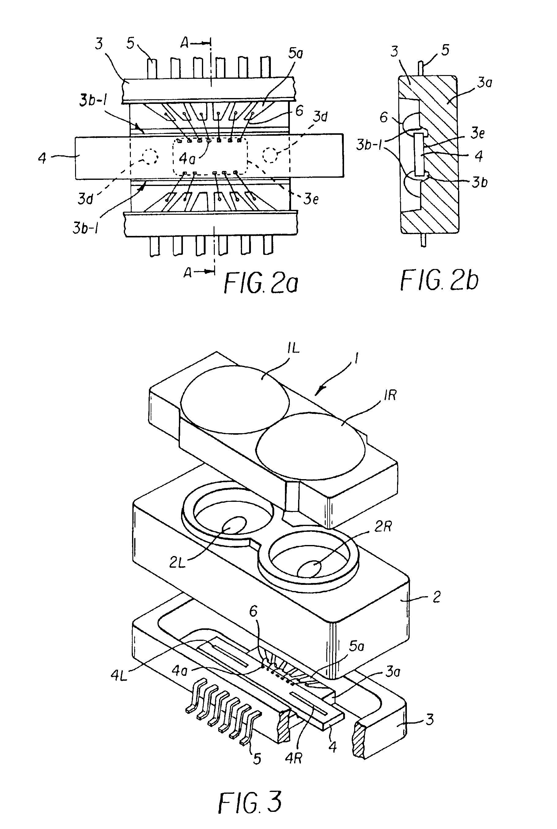
[0025]The invention will be now explained hereinafter with reference to the accompanied drawing figures which illustrate the preferred embodiment of the invention. In the drawing figures which illustrate the preferred embodiment of the invention, the same reference numerals as used in FIGS. 4(a) through 5(b) are used to designate the same constituent elements and their explanations are omitted for the sake of simplicity.

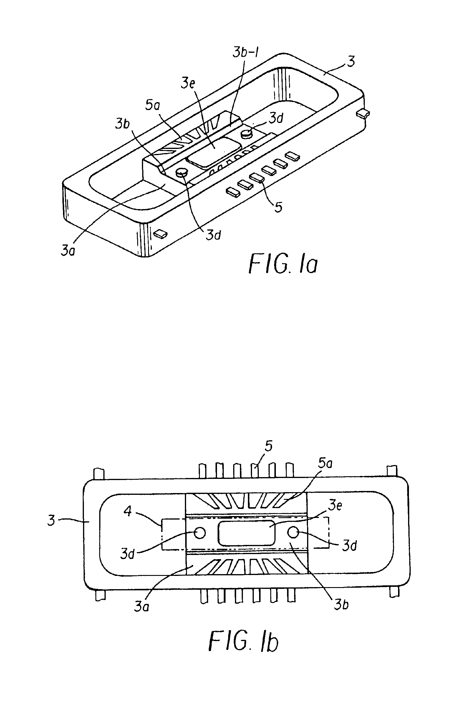
[0026]FIG. 1(a) is a perspective view of a sensor stage according to an embodiment of the invention. FIG. 1(b) is a top plan view of the sensor stage shown in FIG. 1(a). Referring now to these figures, the sensor stage 3 according to the embodiment includes a bottom wall 3a, a U-groove 3b formed in the surface portion of the bottom wall 3a, a rectangular-island-shaped flat pedestal 3e in the central portion of the U-groove 3b, and a pair of pins 3d on both sides of the rectangular pedestal 3e. The pins 3d are aligned in the longitudinal direction of the U-groove 3b. ...


PUM


Abstract

A semiconductor device module is provided that prevents adhesion defects from causing in bonding a semiconductor sensor chip to a sensor stage with an adhesive and improving the reliability thereof. The semiconductor device module includes a sensor stage and a semiconductor optical sensor chip mounted on the sensor stage. The sensor stage includes a U-groove formed in an upper central surface portion of a bottom wall thereof. The sensor chip is bonded to the sensor stage with a thermosetting and UV-curing adhesive coated in the U-groove. The U-groove, includes an island-shaped flat pedestal located at a central bottom portion of the U-groove for mounting the sensor chip thereon. Pins are preferably disposed on both sides of the pedestal to hold the sensor chip horizontally, and the side walls of the U-groove 3b are preferably slanted such that the adhesive coated in the U-groove is prevented from splashing to the outside.

Description

CROSS-REFERENCE TO RELATED APPLICATIONS[0001]The present invention is a continuation-in-part of U.S. patent application Ser. No. 10 / 004,269 filed Oct. 24, 2001, now U.S. Pat. No. 6,583,433, laid open patent application Ser. No. 2002-0,084,432, laid open Jul. 4th, 2002, the disclosure of which is incorporated herein by reference.BACKGROUND OF THE INVENTION[0002]The present invention relates to a semiconductor device module used in a range finder module mounted an automatic focusing camera. Specifically, the present invention relates to the structure of a sensor stage that mounts a semiconductor optical sensor chip thereon.[0003]FIG. 3 is an exploded perspective view showing the module structure of the related range finder disclosed by the present inventors in Japanese patent application No. 2001-328568, on which U.S. patent application Ser. No. 10 / 004,269 is based. Referring now to FIG. 3, the related range finder module includes an optical lens mount 1 including a pair of lenses 1L ...

Claims


Application Information

Patent Timeline
Patent Type & Authority Patents(United States)
IPC IPC(8): G01S17/50G01S17/00G02B7/34
CPCG02B7/34G01S17/50
Inventor SUGIYAMA, OSAMUIZUMI, AKIOYAMAMOTO, TOSHIO
Owner FUJI ELECTRIC CO LTD
Why Eureka
Try Eureka