Memory defect redress analysis treating method, and memory testing apparatus performing the method

a memory defect and defect redress technology, applied in the field of memory defect redress analysis treating method and memory testing apparatus performing method, can solve the problems of increasing the defect rate of ic memories, unable to carry out failure repair analysis and processing at high speed, and increasing the time required to execute the repair analysis and processing for (n+1) memory cell array group. the effect of removing the prior art disadvantages

Inactive Publication Date: 2005-06-14
ADVANTEST CORP
View PDF12 Cites 11 Cited by
  • Summary
  • Abstract
  • Description
  • Claims
  • Application Information

AI Technical Summary

Benefits of technology

[0034]It is an object of the present invention to provide a failure repair analyzing and processing method by which the failure repair analysis and processing for a memory having redundancy structure can be carried out at high speed.
[0035]It is another object of the present invention to provide a memory testing apparatus provided with a failure repair analyzing and processing apparatus that is capable of carrying out at high speed the failure repair analysis and processing for a memory having redundancy structure.
[0047]Moreover, each of the repair analysis units operates independently, and when one repair analysis unit has completed the repair analysis and processing operation for a data bit or memory cell array assigned thereto, it executes the repair analysis and processing operation for the next unprocessed data bit or memory cell array. Accordingly, even if there occurs a delay in completion of the repair analysis and processing operation of one repair analysis unit because it performs the repair analysis and processing for a memory cell array in which many failure memory cells exist and it takes a long time in the repair analysis and processing thereof, the remaining repair analysis unit or units carry out the failure repair analysis and processing for an unprocessed data bit or memory cell array in sequence. As a result, even if a number of failure memory cells exist biasedly in a specified memory cell array, the whole repair analysis and processing time is considerably shortened. Thus, it is possible to remove the prior art disadvantages.

Problems solved by technology

In recent years, a semiconductor memory (particularly, an IC memory) has a tendency that its storage capacity is increased and that its size is miniaturized, and with the increased memory capacity and the miniaturization, a defect rate of IC memories has been increased.
Accordingly, there is a disadvantage that a time required to execute the repair analysis and processing for (N+1) memory cell array groups comes to considerably long.
Accordingly, even there exists only one failure repair analyzing and processing apparatus that takes a long time to carry out the failure repair analysis and processing for a memory under test, the failure repair analysis and processing time for the whole apparatuses comes to the failure repair analysis and processing time for the failure repair analyzing and processing apparatus that has taken the longest time, which results in a shortcoming that the failure repair analysis and processing cannot be carried out at high speed.
Recently, since the storage capacity of a memory is increasing more and more and the number of bits of a memory is also increasing, there has been a tendency that the failure repair analysis and processing time for a memory having redundancy structure is still more increased.

Method used


Image

  • Memory defect redress analysis treating method, and memory testing apparatus performing the method
  • Memory defect redress analysis treating method, and memory testing apparatus performing the method
  • Memory defect redress analysis treating method, and memory testing apparatus performing the method

Examples


Embodiment Construction

[0055]Now, a preferred embodiment of the present invention will be described in detail with reference to FIGS. 1 to 3. The present invention may, however, be embodied in many different forms and should not be construed as limited to the embodiment set forth hereinafter; rather, the embodiment described later on is provided so that this disclosure will be thorough and complete, and will fully convey the scope of the invention to those skilled in the art.

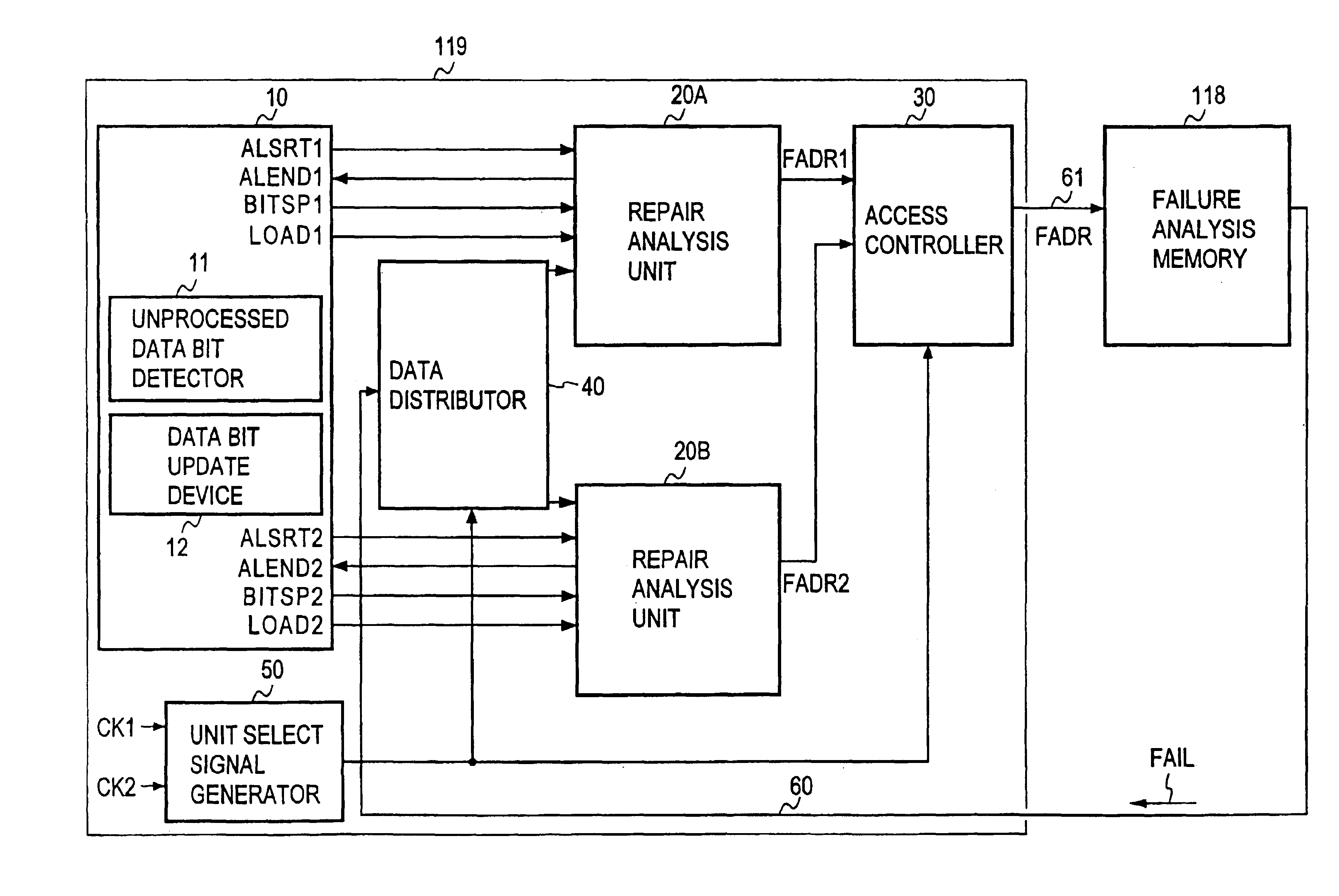
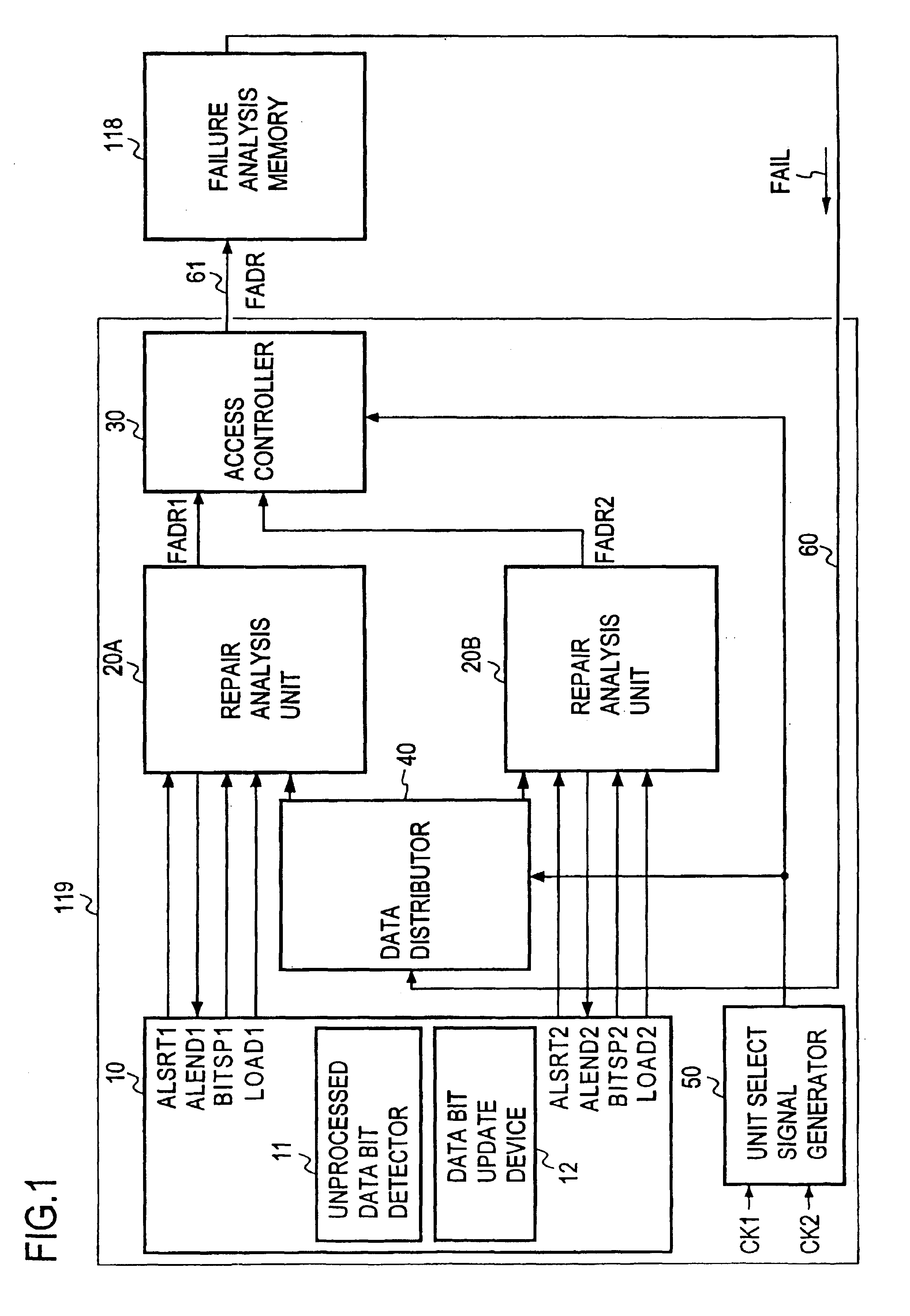
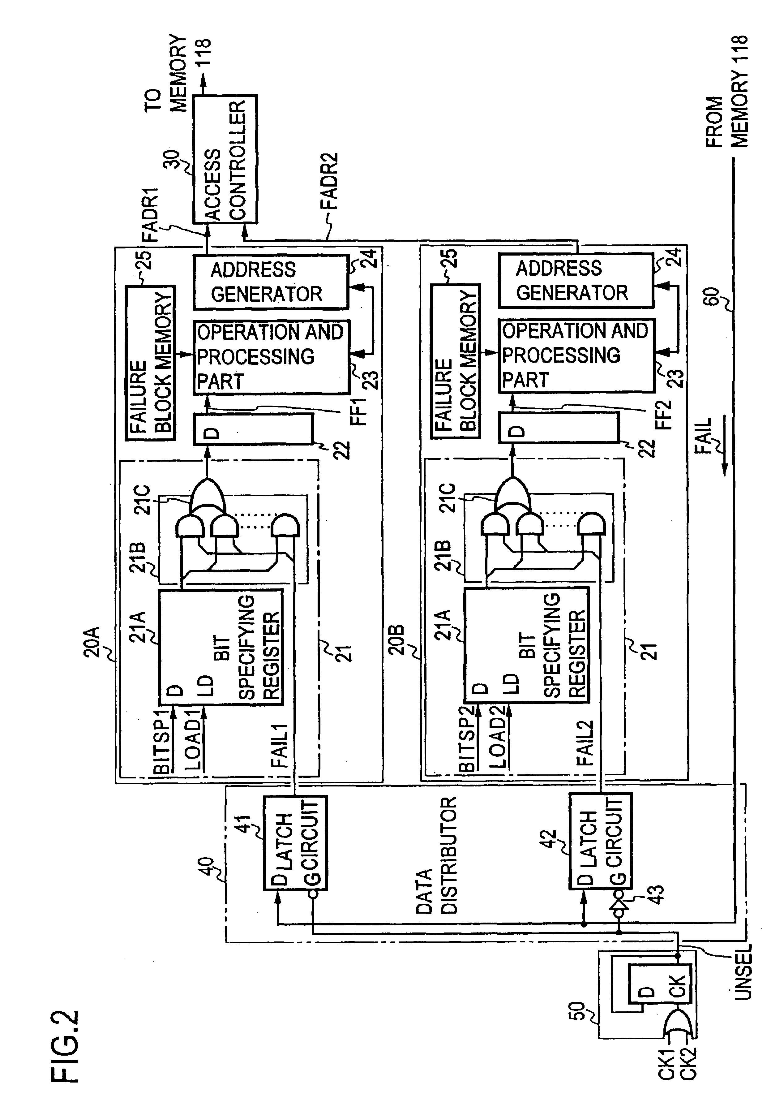
[0056]FIG. 1 is a block diagram showing a rough construction of an embodiment of the memory testing apparatus according to the present invention that is provided with a failure repair analyzing and processing apparatus using a method of analyzing and processing a repair of failure in a memory according to the present invention, and FIG. 2 is a block diagram showing a detailed construction of the failure repair analyzing and processing apparatus shown in FIG. 1. In this memory testing apparatus, a failure analysis memory 118 may be one...


PUM


Abstract

There are provided a failure repair analyzing and processing method and a memory testing apparatus provided with a failure repair analyzing and processing apparatus using this method, that are capable of reducing a time duration required to perform the failure repair analysis and processing for a multi-bit memory having redundancy structure. A plurality of repair analysis units as well as a common failure analysis memory are provided, and these repair analysis units are concurrently operated in parallel with each other, thereby to carry out respective repair analyses and processings for failure memory cells of plural data bits read out from the failure analysis memory in the plural repair analysis units concurrently and in parallel with each other. As a result, a time duration required to execute the failure repair analysis and processing is shortened.

Description

TECHNICAL FIELD[0001]The present invention relates to a method of analyzing and processing a repair of failure in a memory, that comprises the step of analyzing as to whether a failure memory cell or cells existing in a memory having redundancy structure tested by a memory testing apparatus can be repaired or relieved or not, and a memory testing apparatus using the method.BACKGROUND ART[0002]Memory testing apparatuses for testing various types of semiconductor memories including, for example, a memory (IC memory) constructed by a semiconductor integrated circuit (IC) can be classified, roughly, into a memory testing apparatus for testing a memory in wafer state before packaged and a memory testing apparatus for testing a memory after packaged. The memory testing apparatus for testing a memory in wafer state before packaged differs remarkably from the memory testing apparatus for testing a memory after packaged in that the former apparatus is provided with a failure repair processin...

Claims


Application Information

Patent Timeline
Patent Type & Authority Patents(United States)
IPC IPC(8): G11C29/56
CPCG11C29/56G11C2029/5606G11C29/00
Inventor YASUI, TAKAHIRO
Owner ADVANTEST CORP
Why Eureka
Try Eureka