Method for performing an alignment measurement of two patterns in different layers on a semiconductor wafer

a technology of alignment measurement and semiconductor wafer, which is applied in the direction of semiconductor/solid-state device testing/measurement, image enhancement, instruments, etc., to achieve the effect of increasing the yield of the wafer and reducing the time needed

Inactive Publication Date: 2005-06-21
QIMONDA
View PDF9 Cites 21 Cited by
  • Summary
  • Abstract
  • Description
  • Claims
  • Application Information

AI Technical Summary

Benefits of technology

[0011]It is accordingly an object of the invention to provide a method for performing an alignment measurement that overcomes the above-mentioned disadvantages of the heretofore-known devices and methods of this general type and which decreases the time needed for an alignment measurement or overlay measurement of a semiconductor wafer and to increase the wafer yield.
[0028]Since an alignment and overlay quality can be retained or even enhanced due to the selection of exposure fields and their substitutes, the wafer yield is increased and the time spent in system maintenance or repair is advantageously reduced.

Problems solved by technology

For example, this may be due to the obscuring or damaging effects as mentioned above.

Method used


Image

  • Method for performing an alignment measurement of two patterns in different layers on a semiconductor wafer
  • Method for performing an alignment measurement of two patterns in different layers on a semiconductor wafer
  • Method for performing an alignment measurement of two patterns in different layers on a semiconductor wafer

Examples


Embodiment Construction

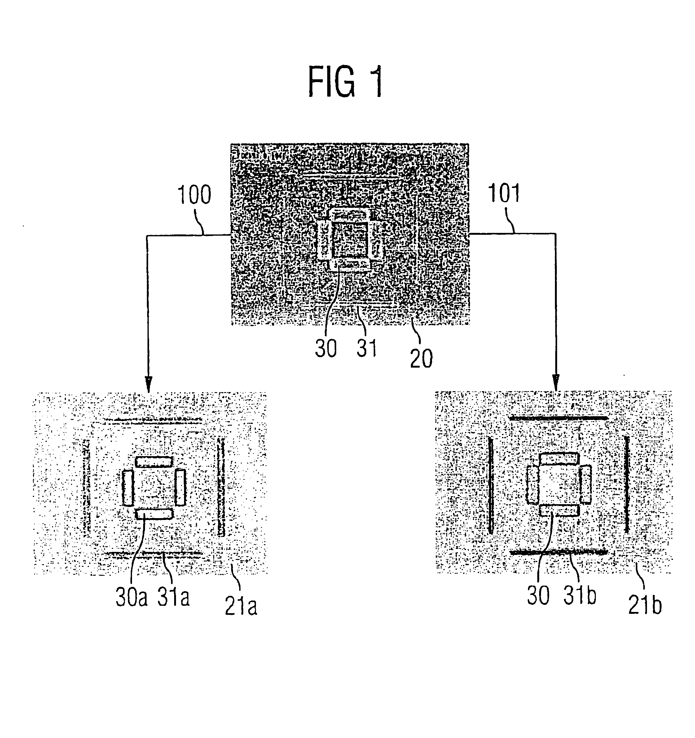
[0039]Referring now to the figures of the drawing in detail and first, particularly, to FIG. 1 thereof, there is shown in the upper portion of the figure an alignment structure 20 embodied as an overlay target to be measured in a metrology tool, which has poor quality due to previous processing steps. The alignment structure 20 is positioned in the upper left corner of the scribeline of each exposure field 2 of a semiconductor wafer 1. In this example the alignment structure 20 consists a) of 4 quadratically arranged twin-trenches formed in a previously structured deep trench layer of a 0.14 μm DRAM-pattern to form a reference target 31, and b) of four smaller equally structured bars in a resist layer, which is the gate contact layer, inside the square of the four twin-trenches, to provide a resist target 30.

[0040]An overlay measurement comprises measuring a deviation of the center of the resist target 30 with respect to the already structured reference target 31 of the previously f...


PUM

PropertyMeasurementUnit
relative distanceaaaaaaaaaa
widthaaaaaaaaaa

Abstract

In an alignment or overlay measurement of patterns on a semiconductor wafer an error that occurs during the measurement in one of a predefined number of alignment structures in an exposure field of a corresponding predefined set of exposure fields can be handled by selecting an alignment structure in a substitute exposure field. The latter exposure field need not be part of the predefined set of exposure fields, that is, an inter-field change may be effected. The number of alignment measurements on a wafer remains constant and the quality is increased. Alternatively, when using another alignment structure in the same exposure field—by effecting an intra-field change—the method becomes particularly advantageous when different minimum structure sizes are considered for the substitute targets. Due to the different selectivity in, say, a previous CMP process, such targets might not erode and do not cause an error in a measurement, thus providing an increased alignment or overlay quality.

Description

CROSS-REFERENCE TO RELATED APPLICATION[0001]This application is a continuation of copending International Application No. PCT / EP02 / 04834, filed May 2, 2002, which designated the United States and was published in English.BACKGROUND OF THE INVENTIONField of the Invention[0002]The invention lies in the semiconductor processing field. More specifically, the present invention relates to a method for measuring an alignment of two patterns in different layers on a semiconductor wafer. A set of exposure fields having a fixed number of fields are selected for the alignment measurement and each of the exposure fields are provided with at least one alignment structure.[0003]Throughout this document the term alignment structure refers to any measurement mark used for identifying absolute or relative positions on a semiconductor wafer, for example alignment marks for aligning a wafer on a stage in an exposure tool or overlay targets for comparing the deviation of two patterns in different layer...

Claims


Application Information

Patent Timeline
Patent Type & Authority Patents(United States)
IPC IPC(8): G03F9/00G03F7/20G06T7/00G06T7/33H01L21/027
CPCG03F7/70633G03F9/7046G03F9/7076G06T7/0004G06T7/0028G06T7/0002G06T2207/30148G06T7/33H01L21/027
Inventor HEINE, ROLFSCHMIDT, SEBASTIANSCHEDEL, THORSTEN
Owner QIMONDA
Why Eureka
Try Eureka