High density DRAM with reduced peripheral device area and method of manufacture
a peripheral device and high density technology, applied in the field of dynamic random access memory (dram) structures, can solve the problems of current manufacturing methods that limit the size of arrays and support circuitry components, and achieve the effect of reducing the area of peripheral transistors that are necessary for mask layout, reducing overall width of peripheral transistors, and less area
- Summary
- Abstract
- Description
- Claims
- Application Information
AI Technical Summary
Benefits of technology
Problems solved by technology
Method used
Image

Examples
Embodiment Construction
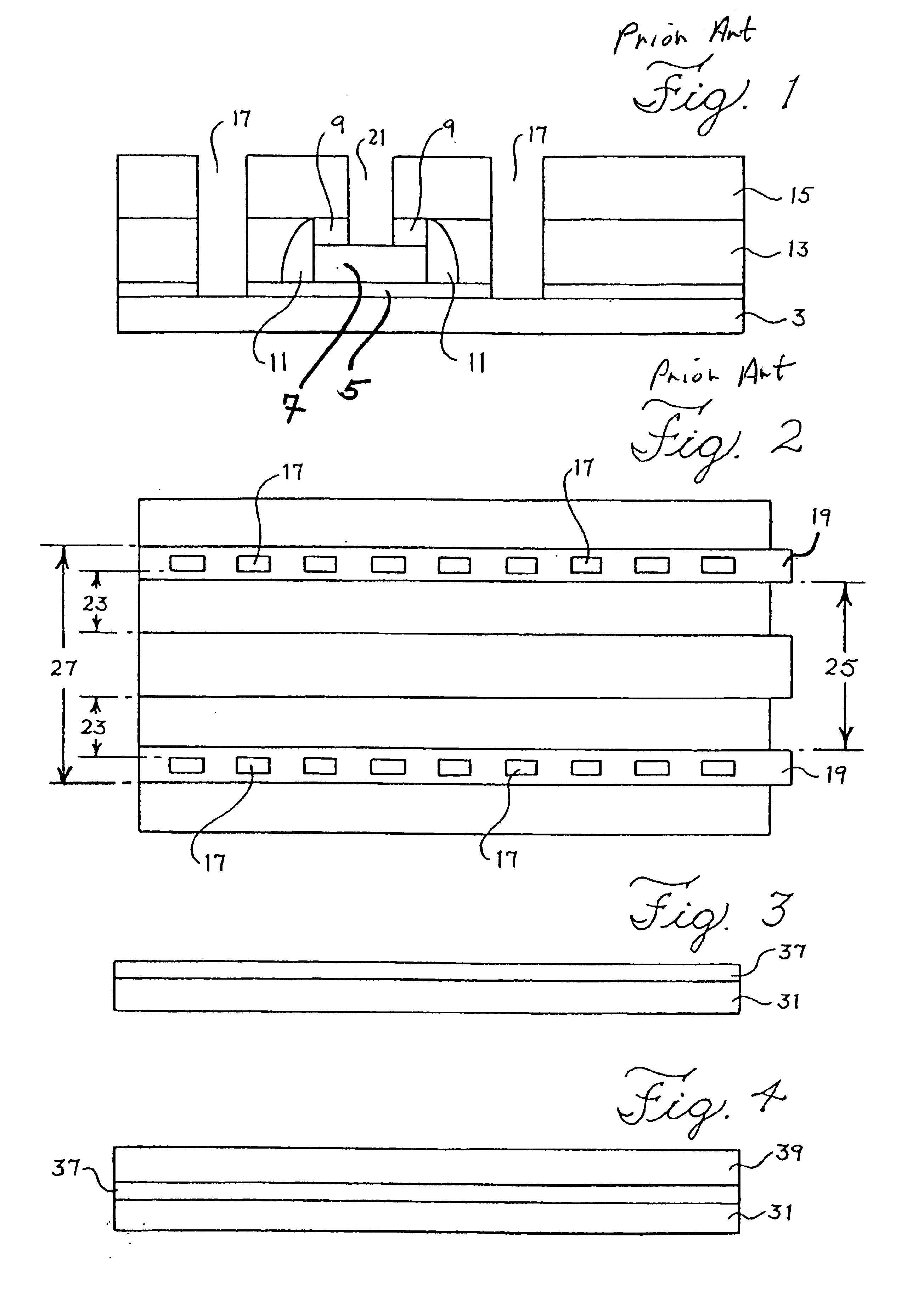
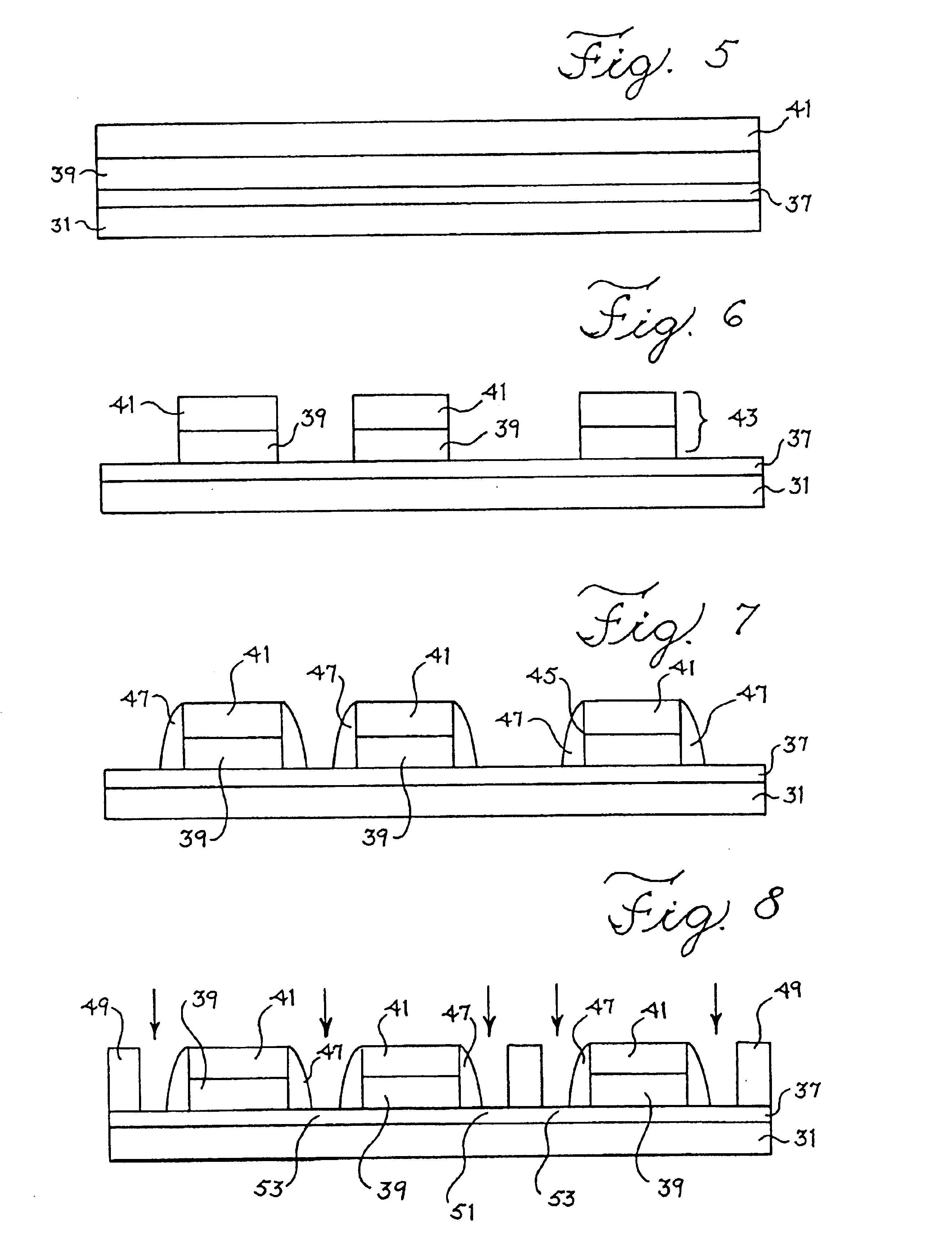
[0018]As is known in the manufacture of silicon integrated circuits, it is conventional to do the processing on a relatively large silicon wafer after which the wafer is diced into individual silicon chips, which include the desired integrated circuit. For convenience, the description of the method of the present invention will be primarily in terms of a single chip, which is formed into a single DRAM. However, it should be appreciated that the method is equally applicable to wide scale production of large silicon wafers.
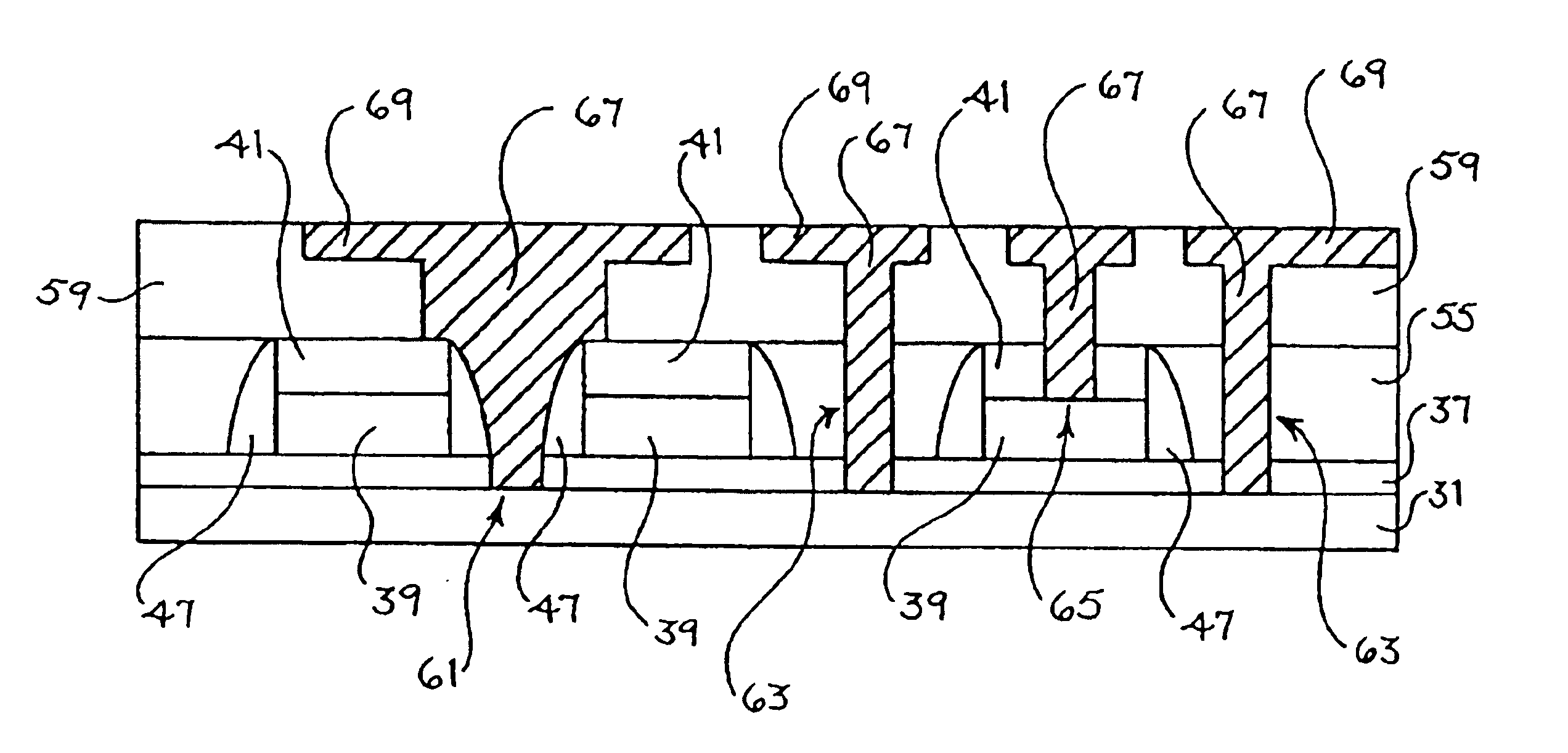
[0019]FIG. 3 shows a portion of a substrate 31, which comprises an array portion where N-MOSFETs are formed for the memory cells of a DRAM, and a periphery portion where N-MOSFETs and P-MOSFETS are formed for the support circuitry of the DRAM. Typically, the support circuitry is concentrated in regions that border the area where the memory cells are concentrated. The substrate 31 may be monocrystalline silicon or any other suitable semiconductor substrate material.
[...
PUM
 Abstract
Description
Claims
Application Information
 - R&D
- Intellectual Property
- Life Sciences
- Materials
- Tech Scout
- Unparalleled Data Quality
- Higher Quality Content
- 60% Fewer Hallucinations
Browse by: Latest US Patents, China's latest patents, Technical Efficacy Thesaurus, Application Domain, Technology Topic, Popular Technical Reports.
© 2025 PatSnap. All rights reserved.Legal|Privacy policy|Modern Slavery Act Transparency Statement|Sitemap|About US| Contact US: help@patsnap.com