Electronic assembly having semiconductor component with polymer support member and method of fabrication
What is Al technical title?
Al technical title is built by PatSnap Al team. It summarizes the technical point description of the patent document.
a technology of support member and semiconductor, applied in the field of semiconductor components, can solve problems such as fatigue failure of contact balls, adversely affecting assembly reliability, and compounding of problems
Inactive Publication Date: 2005-06-21
MICRON TECH INC
View PDF29 Cites 63 Cited by
Summary
Abstract
Description
Claims
Application Information
AI Technical Summary
This helps you quickly interpret patents by identifying the three key elements:
Problems solved by technology
Method used
Benefits of technology
[0019]In accordance with the present invention, an improved semiconductor component, and a method for fabricating the component are provided. The semiconductor comp...
Problems solved by technology
One factor that can adversely affect the reliability of the assembly 22A during operation in different customer environments is fatigue failure of the contact ball 10A, particularly at t...
Method used
Image
Click on the blue label to locate the original text in one second.
Reading with bidirectional positioning of images and text.
Examples
Embodiment Construction
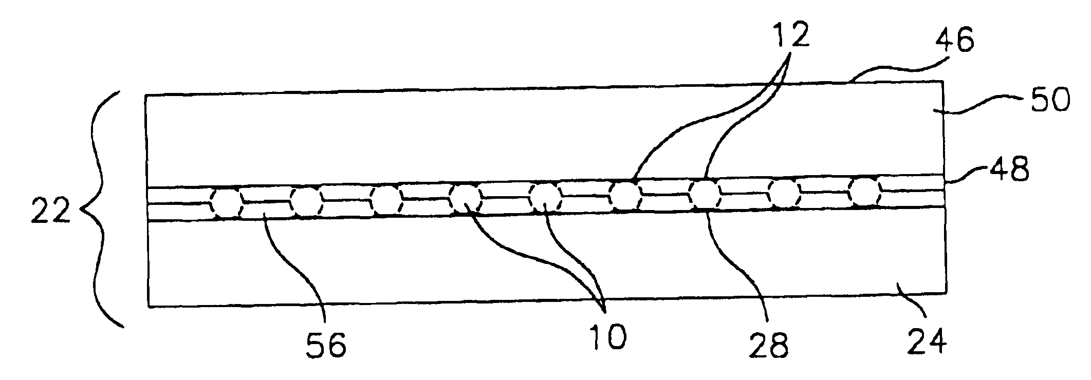
[0044]Referring to FIGS. 2A and 2B, a semiconductor component 46 constructed in accordance with the invention is illustrated. As used herein the term “semiconductor component” refers to an element, or an assembly, that includes a semiconductor die. By way of example, the semiconductor component 46 can comprise a chip scale package, a BGA device, a bare semiconductor die, a semiconductor wafer containing semiconductor dice, or a panel or wafer containing semiconductor packages.
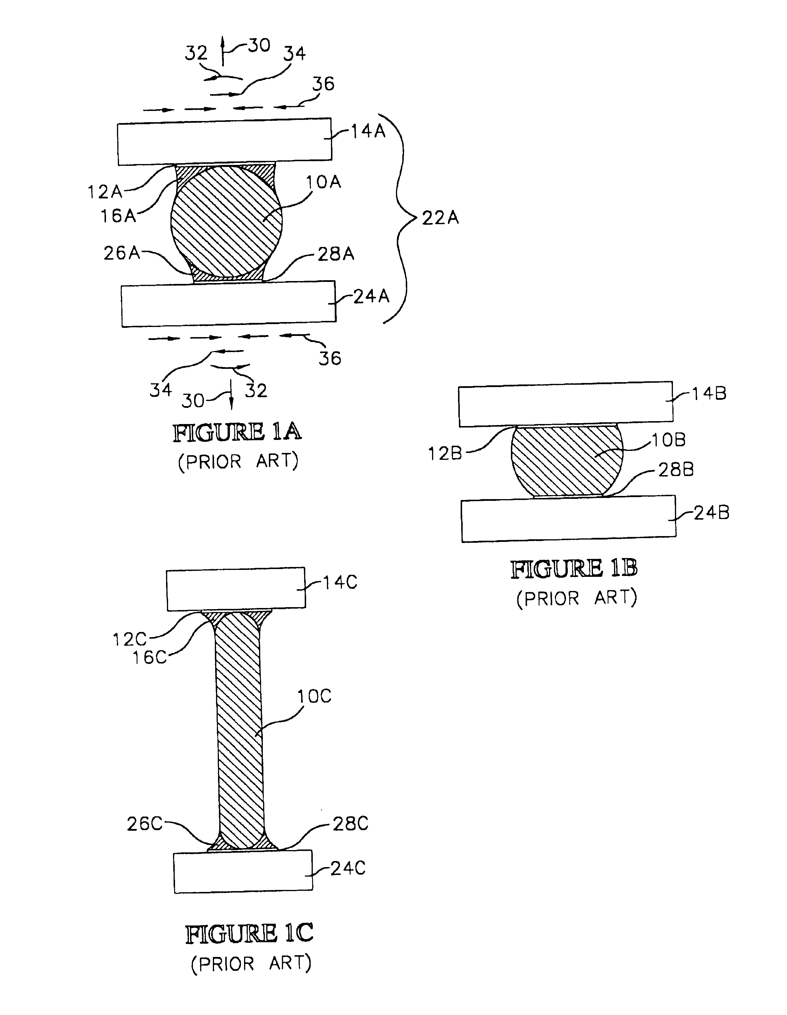
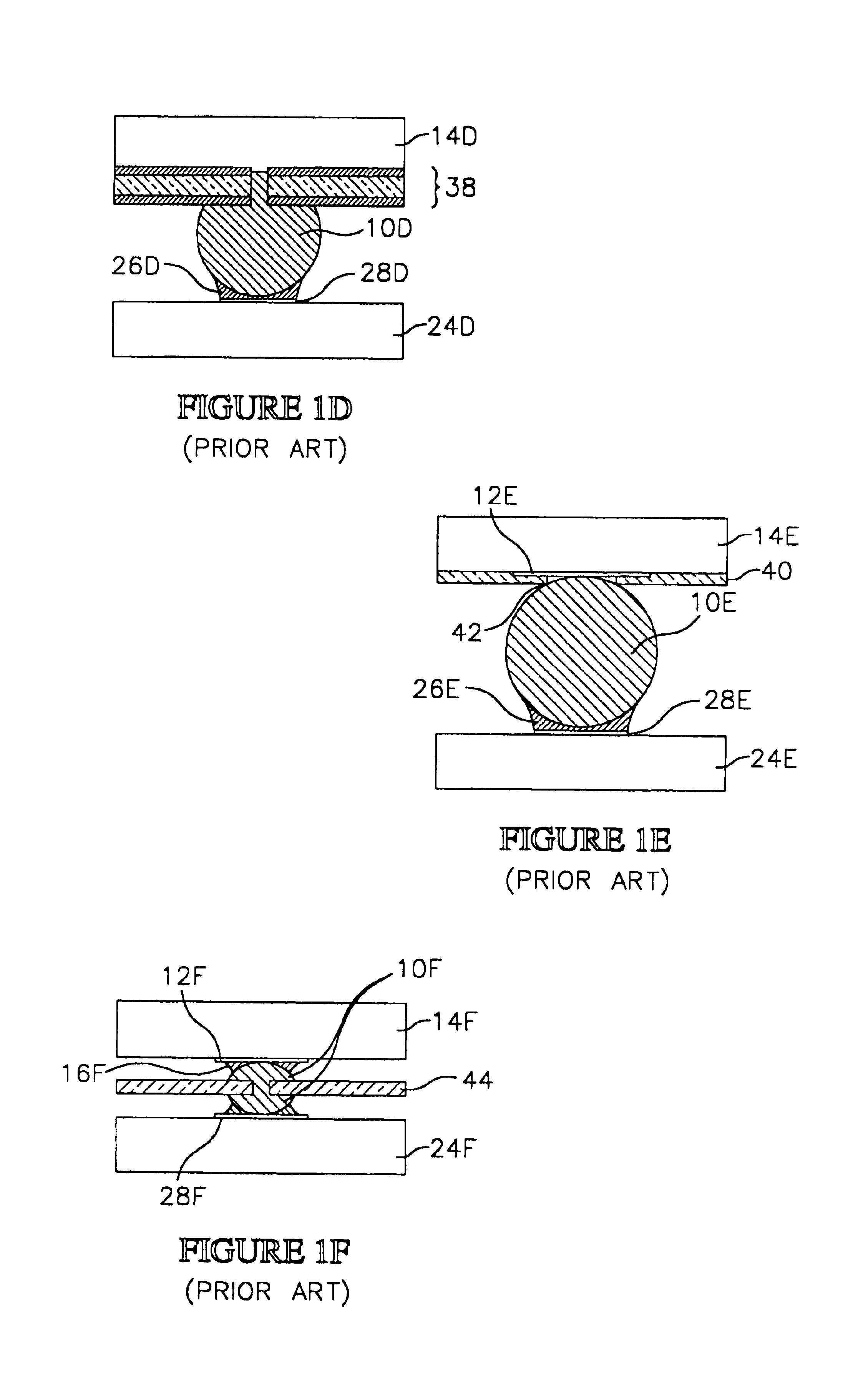
[0045]The component 46 includes a substrate 50, and a plurality of bonding pads 12 and external contacts 10 formed on a surface 52 of the substrate 50. Representative materials for the component substrate 50 include ceramic, silicon, and glass filled plastics such as FR-4. Representative materials for the bonding pads 12 include molybdenum, copper and nickel. As will be further explained, the external contacts 10 can comprise any of the embodiments shown in FIGS. 1A-1F. The external contacts 10 are in electrica...
PUM
Abstract
A semiconductor component includes a substrate, bonding pads on the substrate, and external contacts bonded to the bonding pads. Exemplary external contacts include solder balls, solder bumps, solder columns, TAB bumps and stud bumps. Preferably the external contacts are arranged in a dense array, such as a ball grid array (BGA), or fine ball grid array (FBGA). The component also includes a polymer support member configured to strengthen the external contacts, absorb forces applied to the external contacts, and prevent separation of the external contacts from the bonding pads. In a first embodiment, the polymer support member comprises a cured polymer layer on the substrate, which encompasses the base portions of the external contacts. In a second embodiment, the polymer support member comprises support rings which encompass the base portions of the external contacts. In either embodiment the polymer support member transfers forces applied to the external contacts away from the interface with the bonding pads, and into the center of the contacts.
Description
CROSS REFERENCE TO RELATED APPLICATIONS[0001]This application is a continuation of Ser. No. 09 / 653,366 filed Sep. 1, 2000 now U.S. Pat. No. 6,756,253, which is a division of Ser. No. 09 / 440,380 filed Nov. 15, 1999, U.S. Pat. No. 6,180,504 B1, which is a division of Ser. No. 09 / 384,783 filed Aug. 27, 1999, U.S. Pat. No. 6,118,179.FIELD OF THE INVENTION[0002]This invention relates generally to semiconductor manufacture, and more particularly to an improved semiconductor component, and to a method for fabricating the component.BACKGROUND OF THE INVENTION[0003]Semiconductor components, such as packages, dice and wafers can include external contacts in the form of solder contact balls. The contact balls are in electrical communication with integrated circuits, and other electrical elements, contained on the components. For some components, such as chip scale packages and BGA packages, the contact balls can be arranged in a dense grid array, such as a ball grid array (BGA), or a fine ball...
Claims
Application Information
Patent Timeline
Application Date:The date an application was filed.
Publication Date:The date a patent or application was officially published.
First Publication Date:The earliest publication date of a patent with the same application number.
Issue Date:Publication date of the patent grant document.
PCT Entry Date:The Entry date of PCT National Phase.
Estimated Expiry Date:The statutory expiry date of a patent right according to the Patent Law, and it is the longest term of protection that the patent right can achieve without the termination of the patent right due to other reasons(Term extension factor has been taken into account ).
Invalid Date:Actual expiry date is based on effective date or publication date of legal transaction data of invalid patent.