Portable microdisplay system

a micro-display and display panel technology, applied in the field of portable micro-display systems, can solve the problems of increasing the complexity of the integrated circuit of the display, limiting the further circuit processing to low temperatures, and reducing the cost and complexity of high-resolution displays, so as to achieve the effect of reducing size and cos

Inactive Publication Date: 2005-06-21
KOPIN CORPORATION
View PDF202 Cites 223 Cited by
  • Summary
  • Abstract
  • Description
  • Claims
  • Application Information

AI Technical Summary

Benefits of technology

[0008]In accordance with the invention, the cost and complexity of high resolution displays are significantly reduced by fabricating

Problems solved by technology

These materials are limited as they use silicon that is already on glass, which generally restricts further circuit processing to low

Method used


Image

  • Portable microdisplay system
  • Portable microdisplay system
  • Portable microdisplay system

Examples


Embodiment Construction

High Resolution Active Matrix Microdisplay

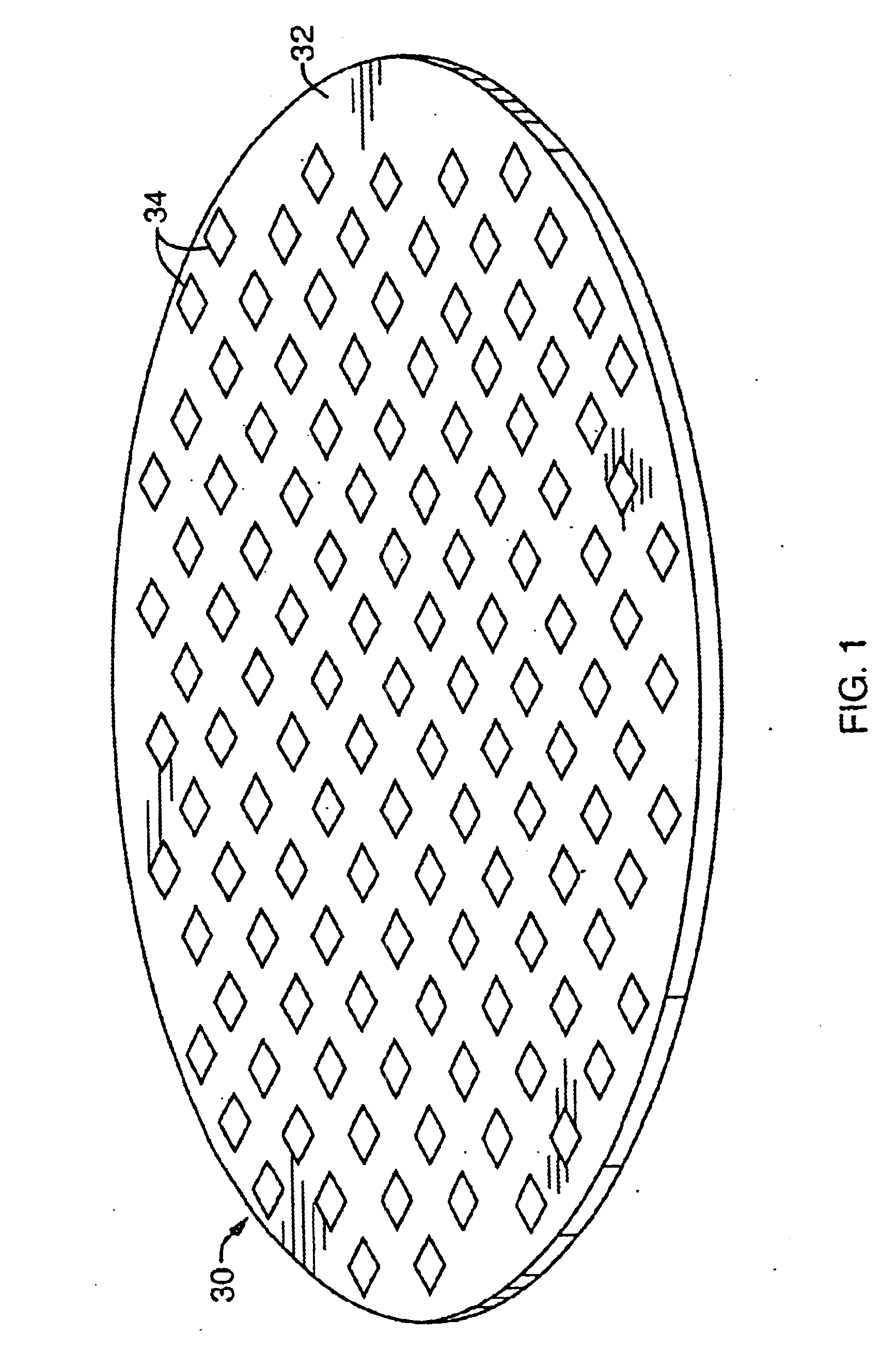
[0116]A preferred embodiment of the invention utilizes a process of making a plurality of flat panel displays 30 in which a large number of active matrix arrays 34 are fabricated on a single wafer 32 as illustrated in connection with FIG. 1.

[0117]The number of displays fabricated on a single wafer depends upon the size of the wafer and the size of each display. A preferred embodiment of the invention, for example, uses a high resolution display having an imaging area of the display with a diagonal of 0.24 inches or less. The active display area is 4.8 mm×3.6 mm and has a total display dimension of 11.8 mm×6.8 mm. 120 separate displays can be fabricated on a single five inch wafer.

[0118]By fabricating a large number of small high resolution displays on a single wafer, the manufacturing yield can be substantially increased and the cost per display can be substantially reduced.

[0119]To obtain monochrome or color sequential resolutions of at lea...


PUM


Abstract

An active matrix color crystal display has an active matrix circuit, a counterelectrode panel and an interposed layer of liquid crystal. The active matrix display is located in a portable microdisplay system that has a display computer that generates images to be displayed on the liquid crystal display and connected to the active matrix liquid crystal display. A data link transmits data at a rate of speed of greater than 200 Mbytes per second in series for at least a portion between the display computer and the active matrix liquid crystal display. In a preferred embodiment, the display system has a randomizing device that alternates the amplifier through which an analog video signal passes.

Description

RELATED APPLICATION(S)[0001]This application is a Continuation-in-Part of U.S. application Ser. No. 09 / 066,061 filed on Apr. 24, 1998 which is a Continuation-in-Part of U.S. application Ser. No. 09 / 004,706 filed on Jan. 8, 1998 now U.S. Pat. No. 6,476,784 which is a Continuation-in-Part of U.S. application Ser. No. 08 / 961,744 filed Oct. 31, 1997, now U.S. Pat. No. 6,552,704 the entire contents of which are incorporated herein by reference.BACKGROUND OF THE INVENTION[0002]Flat-panel displays are being developed which utilize liquid crystals or electroluminescent materials to produce high quality images. These displays are expected to supplant cathode ray tube (CRT) technology and provide a more highly defined television picture or computer monitor image. The most promising route to large scale high quality liquid crystal displays (LCDs), for example, is the active-matrix approach in which thin-film transistors (TFTs) are co-located with LCD pixels. The primary advantage of the active...

Claims


Application Information

Patent Timeline
IPC IPC(8): G06F1/16G06F3/14G09G3/36G09G3/34H04N9/30H04N9/12G02F1/133G02F1/136G02F1/1368G09G3/20
CPCG06F1/1616H04N9/30G06F1/163G06F1/1632G06F1/1637G06F1/1656G06F1/1662G06F1/1686G06F1/1698G09G3/3406G09G3/3413G09G3/3659G06F1/1626G09G2310/0235G09G2310/024G09G2310/08G09G2320/041G09G2320/0633G09G2320/064G09G2330/021
Inventor ZAVRACKY, MATTHEWJACOBSEN, JEFFREYHERRMANN, FREDERICK P.CHERN, WEN-FOOONG, HIAP L.FAN, JOHN C. C.TSAUR, BOR-YEURICHARD, ALANGALE, RONLO, JASONPOMBO, STEPHEN A.BUMGARDNER, RODNEY
Owner KOPIN CORPORATION
Why Eureka
Try Eureka