Semiconductor device

a semiconductor and device technology, applied in the direction of semiconductor devices, semiconductor/solid-state device details, electrical devices, etc., can solve the problems of increasing material costs, and achieve the effect of satisfying heat conductivity, and improving heat dissipation characteristics

Inactive Publication Date: 2005-07-05
MITSUBISHI ELECTRIC CORP
View PDF26 Cites 61 Cited by
  • Summary
  • Abstract
  • Description
  • Claims
  • Application Information

AI Technical Summary

Benefits of technology

[0019]Further, as the ceramic substrate is provided to the metal block, the ceramic substrate may be responsible for a dielectric breakdown voltage. As a result, the material for the jointing material can be selected in terms of heat conductivity without the need of considering dielectric breakdown voltage.
[0030]In the semiconductor device according to the eighth aspect of the present invention, as a gap between the metal block and the semiconductor element becomes wider as a distance from a center of the semiconductor element becomes longer, the thickness of the jointing material is greater in the periphery of the semiconductor element than the thickness at the center of the same. As a result, the amount of cracks can be reduced.

Problems solved by technology

However, as aluminum nitride is more costly than alumina, increase in material cost has been caused.

Method used


Image

  • Semiconductor device
  • Semiconductor device
  • Semiconductor device

Examples


Embodiment Construction

[0042]First Preferred Embodiment

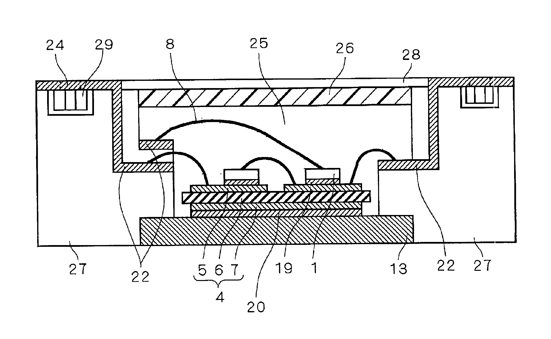
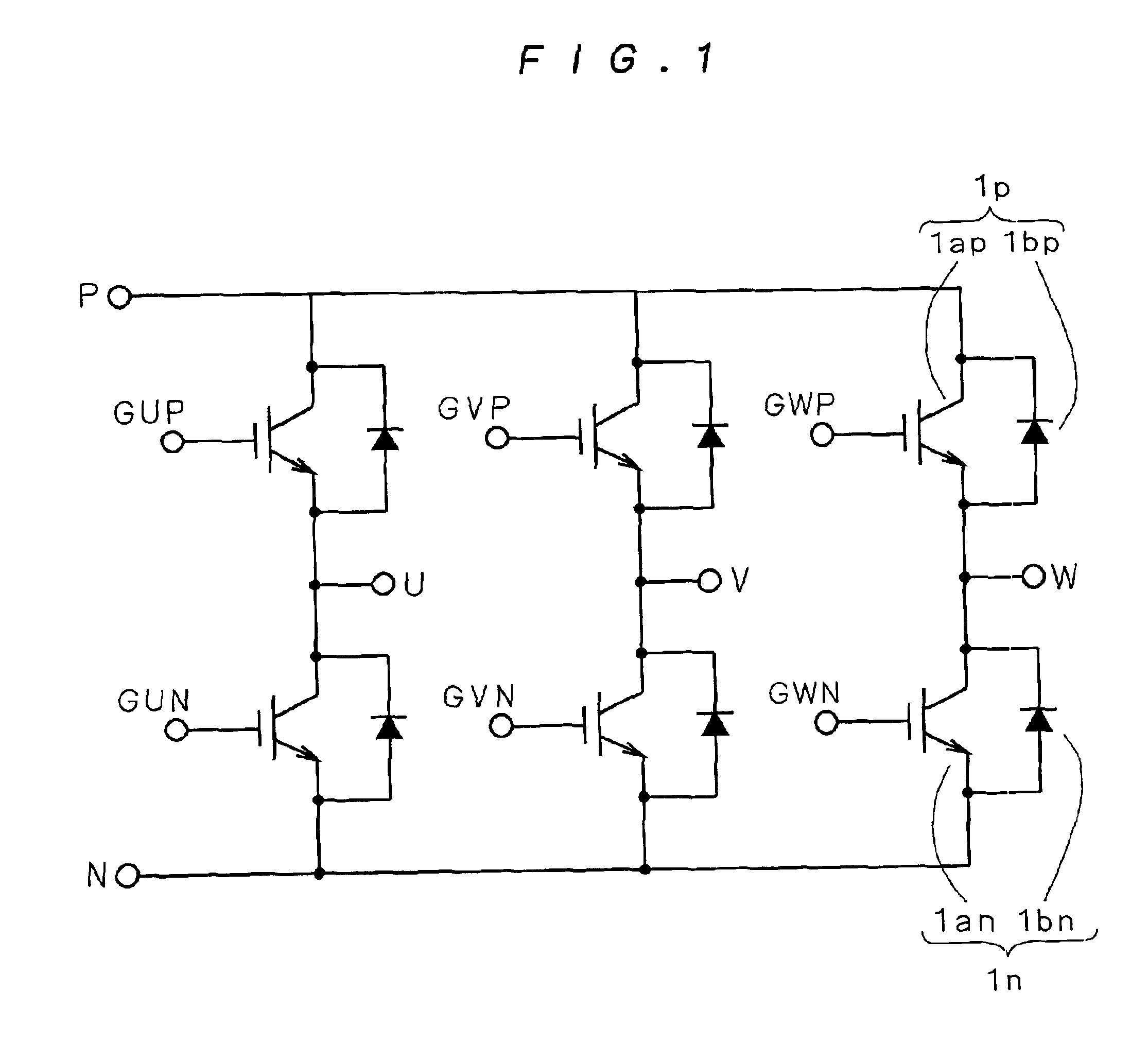
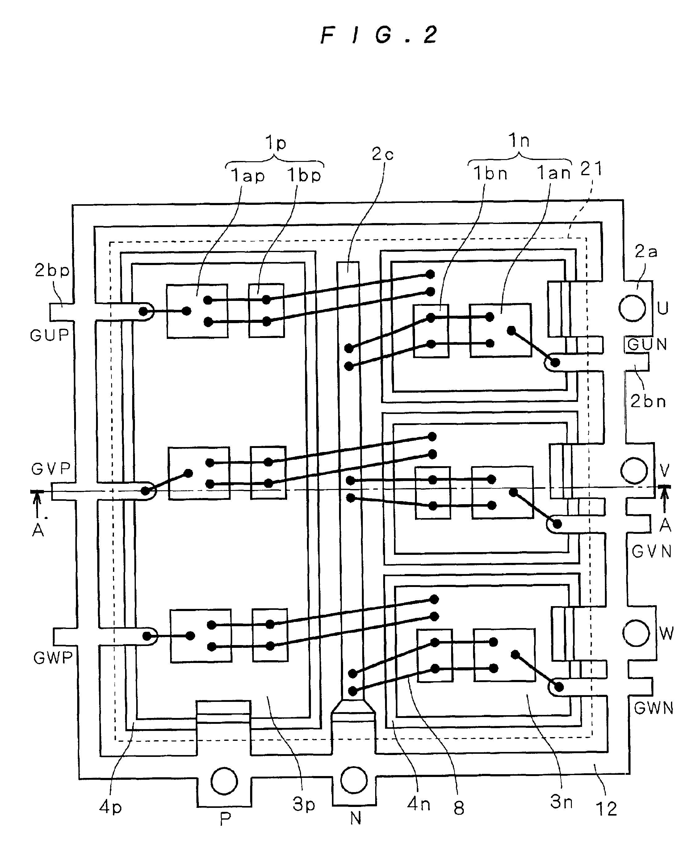
[0043]FIG. 1 is a circuit diagram showing a semiconductor device according to the first preferred embodiment. As shown in FIG. 1, the semiconductor device according to the first preferred embodiment consists of a three-phase inverter circuit, for example. More particularly, output terminals U, V and W may be connected to an AC motor. Input terminals P and N may be directly connected to a DC power supply or to an output of a power rectifier circuit for generating a DC voltage from a commercial power supply. A power element 1p provided on the P side includes an IGBT 1ap and a diode 1bp connected in inverse-parallel connection to the IGBT 1ap. A power element in provided on the N side includes an IGBT 1an and a diode 1bn connected in inverse-parallel connection to the IGBT 1an. The structure connecting the power element 1p and the power element 1n in series is called as arm. The semiconductor device according to the first preferred embodiment includes th...


PUM

PropertyMeasurementUnit
thicknessaaaaaaaaaa
diameteraaaaaaaaaa
diameteraaaaaaaaaa

Abstract

It is an object to provide a semiconductor device having an improved heat dissipation characteristic. A power element is mounted on and jointed and to a metal block through a jointing material. An insulating substrate includes a ceramic substrate and metal layers formed on both surfaces of the ceramic substrate and having thicknesses equal to each other. The metal block and the insulating substrate are provided per insulation unit of the power element. The metal layer of the insulating substrate is joined to a surface of the metal block through a jointing material opposite to a surface thereof for forming the power element. An electrode terminal is attached to a surface of the metal block having a power element joined thereto through ultrasonic junction and the like. Electrode terminals are connected to electrodes of the power element through aluminum wires. The power element, the electrode terminals and the metal block are sealed with a resin package while the metal layer of the insulating substrate remains exposed. An external heat dissipator is attached to the exposed metal layer of the insulating substrate.

Description

BACKGROUND OF THE INVENTION[0001]1. Field of the Invention[0002]The present invention is directed to a structure of a semiconductor device. More particularly, it is directed to a structure of a power semiconductor device used for power control.[0003]2. Description of the Background Art[0004]FIG. 10 is a cross-sectional view schematically showing the structure of a power semiconductor device in the background art. The power semiconductor device in the background art includes power elements 1, a base plate 13, an insulating substrate 4, a case 27 having electrode terminals 22 attached thereto and a cover 28.[0005]The insulating substrate 4 consists of a ceramic substrate 6 made of alumina, aluminum nitride or silicon nitride, for example, and metal layers 5, 7 formed on both surfaces of the ceramic substrate 6. The power element 1 is joined onto the metal layer through solder 19. Further, a circuit pattern is formed on the metal layer 5. The base plate 13 made of copper or the like ac...

Claims


Application Information

Patent Timeline
Patent Type & Authority Patents(United States)
IPC IPC(8): H01L23/495H01L23/433H01L23/48H01L23/34H01L23/36H01L23/373
CPCH01L23/4334H01L23/49575H01L24/32H01L24/49H01L24/45H01L2224/45124H01L2224/48091H01L2224/48137H01L2224/48247H01L2224/49175H01L2224/73265H01L2924/01004H01L2924/01005H01L2924/01013H01L2924/01014H01L2924/01015H01L2924/0102H01L2924/01029H01L2924/01042H01L2924/01074H01L2924/01082H01L2924/13055H01L2924/19043H01L2924/19107H01L2924/00014H01L2224/32225H01L2224/32245H01L2924/01023H01L2924/01033H01L2924/01068H01L2924/014H01L24/48H01L2924/00H01L2924/0132H01L2924/3512H01L2224/48227H01L2924/00012H01L2924/12041H01L2224/48139H01L2224/45015H01L2924/351H01L2924/15787H01L24/73H01L2924/181H01L2224/49113H01L2224/83385H01L2224/48096H01L2224/49111
Inventor SHINOHARA, TOSHIAKI
Owner MITSUBISHI ELECTRIC CORP
Why Eureka
Try Eureka