Structure and method for forming a trench MOSFET having self-aligned features

a technology of trench mosfet and self-aligning features, which is applied in the direction of semiconductor devices, semiconductor/solid-state device details, electrical apparatus, etc., can solve the problems of reducing the cell pitch of mosfets, reducing the cell pitch further, and reducing any of these dimensions without complicating the process technology

Inactive Publication Date: 2005-07-12
SEMICON COMPONENTS IND LLC
View PDF283 Cites 104 Cited by
  • Summary
  • Abstract
  • Description
  • Claims
  • Application Information

AI Technical Summary

Problems solved by technology

However, reducing the cell pitch of MOSFETs is limited by the particulars of the MOSFET cell structure and the specific process recipe used to manufacture the MOSFET.
Reducing the cell pitch is made further difficult by such limitations of the manufacturing process technology as the minimum critic

Method used


Image

  • Structure and method for forming a trench MOSFET having self-aligned features
  • Structure and method for forming a trench MOSFET having self-aligned features
  • Structure and method for forming a trench MOSFET having self-aligned features

Examples


Embodiment Construction

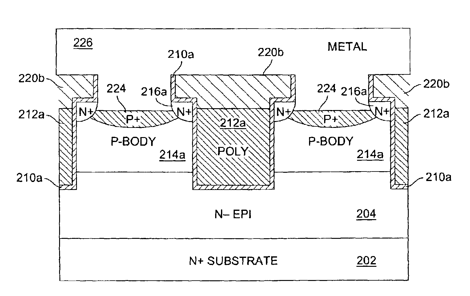
[0023]In accordance with the present invention, a structure and method for forming a trench MOSFET having self-aligned features which result in cell pitch reduction without increasing the process complexity are disclosed. In one embodiment, trenches are formed in an epitaxial layer in such manner that the trench sidewalls fan out near the top of the trench over source regions. An insulating layer formed along a top portion of each trench together with the source regions define the contact openings between adjacent trenches for contacting the source and body regions. This structure and method of forming the trenches leads to a MOSFET which has source regions and contact openings self-aligned to the trenches. This in turn enables the 2D portion of the cell pitch of prior art MOSFET 100 (FIG. 1) to be eliminated and the dimension B to be reduced to thus obtain a reduced cell pitch without introducing any process complexities

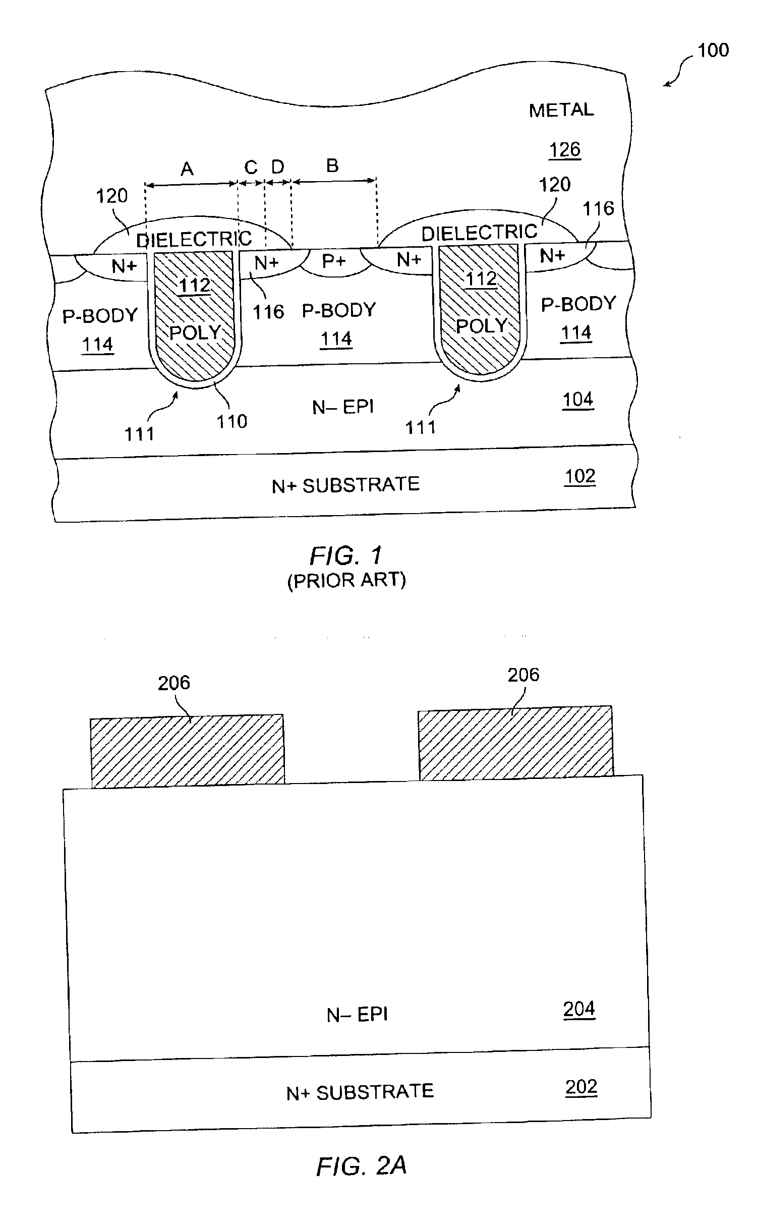
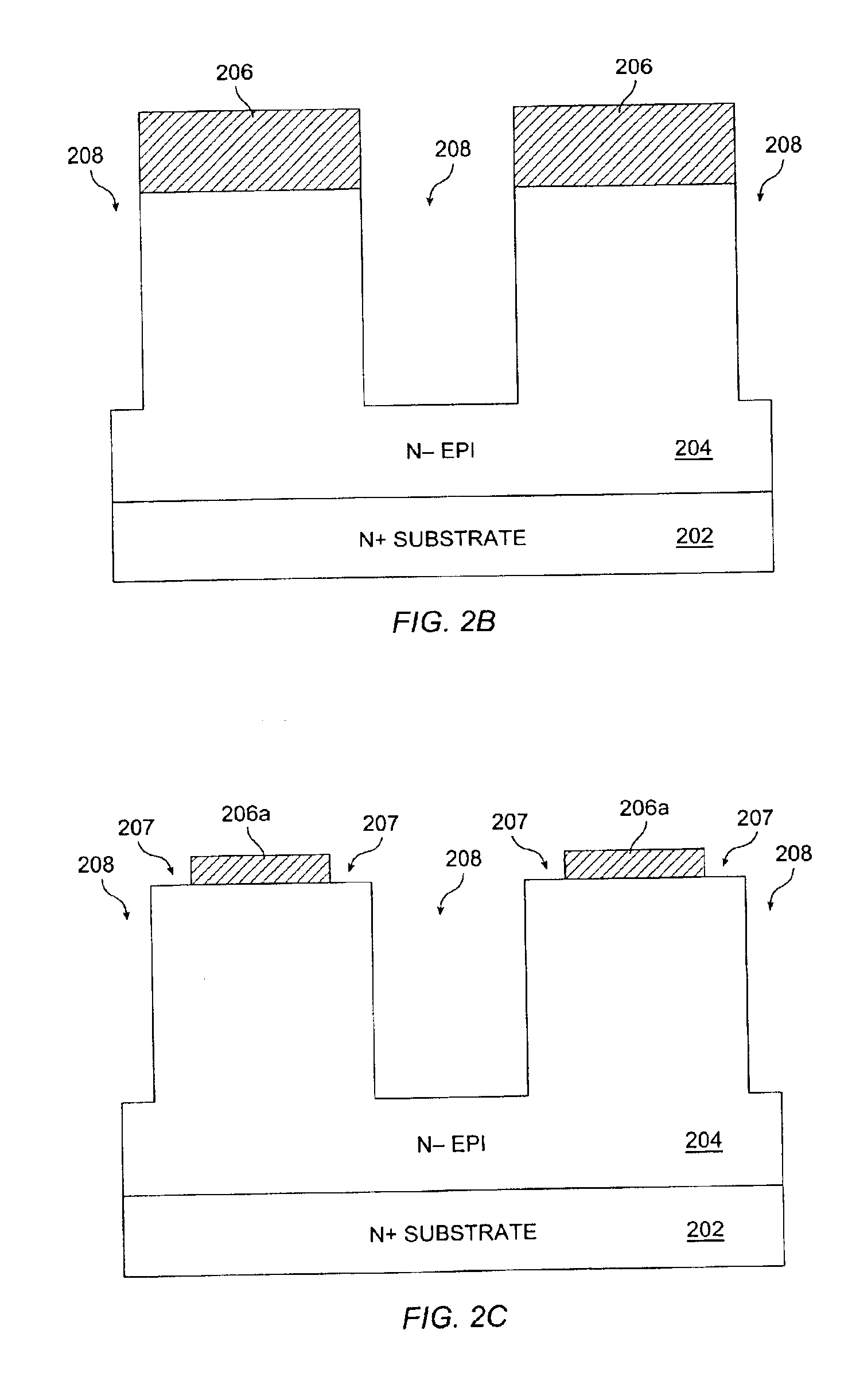
[0024]FIGS. 2A-2K are cross-section views at different stages ...


PUM


Abstract

In accordance with an embodiment of the present invention, a semiconductor device is formed as follows. An exposed surface area of a silicon layer where silicon can be removed is defined. A portion of the silicon layer is removed to form a middle section of a trench extending into the silicon layer from the exposed surface area of the silicon layer. Additional exposed surface areas of the silicon layer where silicon can be removed are defined. Additional portions of the silicon layer are removed to form outer sections of the trench such that the outer sections of the trench extend into the silicon layer from the additional exposed surface areas of the silicon layer. The middle section of the trench extends deeper into the silicon layer than the outer sections of the trench.

Description

BACKGROUND OF THE INVENTION[0001]The present invention relates to semiconductor MOSFET technology and more particularly to a trench MOSFET having self-aligned features.[0002]Power MOSFETs (metal oxide semiconductor field effect transistors) are well known in the semiconductor industry. One variety of power MOSFETs is the vertically-conducting trench MOSFET. A cross-section view of such a MOSFET is shown in FIG. 1. MOSFET 100 has trenches 111 each including a polysilicon gate 112 insulated from body regions 114 by a gate dielectric 110. Source regions 116 flank each side of trenches 111. Dielectric layer 120 insulates gates 112 from overlying metal layer 126. Substrate region 102 forms the drain of MOSFET 100.[0003]When MOSFET 100 is biased in the on state, current flows vertically between source regions 116 and substrate 102. The current capability of MOSFET 100 in the on state is a function of the drain to source resistance (Rdson). To improve the current capability of the MOSFET, ...

Claims


Application Information

Patent Timeline
IPC IPC(8): H01L21/336H01L29/78H01L21/02H01L29/66H01L29/417
CPCH01L29/7813H01L29/41766Y10S257/905H01L29/7802H01L21/18
Inventor HERRICK, ROBERTLOSEE, BECKYPROBST, DEAN
Owner SEMICON COMPONENTS IND LLC
Why Eureka
Try Eureka