Method for forming nanotube semiconductor devices

a technology of nanotubes and semiconductor devices, applied in the direction of semiconductor devices, electrical equipment, nanotechnology, etc., can solve the problems of slow switching speed of sgt, complex and expensive sgt process, and reduced sgt switching speed, so as to achieve uniform doping concentration and charge balance in operation

Active Publication Date: 2011-03-22
ALPHA & OMEGA SEMICON INC
View PDF14 Cites 46 Cited by
  • Summary
  • Abstract
  • Description
  • Claims
  • Application Information

AI Technical Summary

Problems solved by technology

Consequently, vertical MOSFETs are associated with slower switching speed.
Furthermore, Inter Poly Dielectric (IPD) and trench etch (side wall angle) unit step processes makes SGT process complex and expensive.
Additionally, increased output capacitance and resistance of the shielded gate poly silicon will slow down switching speed of SGT.
That is, the dopant concentration is not uniform across the drain drift region and has variation in the horizontal and vertical direction across the drain drift region.

Method used


Image

  • Method for forming nanotube semiconductor devices
  • Method for forming nanotube semiconductor devices
  • Method for forming nanotube semiconductor devices

Examples


first embodiment

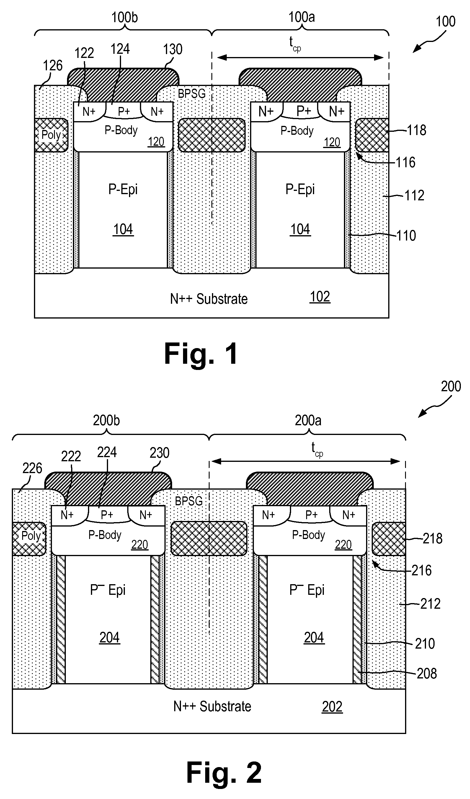
[0051]FIG. 1 is a cross-sectional view of a vertical trench MOSFET device according to the present invention. Referring to FIG. 1, an N-type vertical trench MOSFET device (“NMOS transistor”) 100 is formed in an array of parallely connected transistor cells 100a and 100b. A desired number of transistor cells are used to form the array to realize an NMOS transistor 100 having the desired breakdown voltage and Rdson (drain-to-source “On” resistance) characteristic. The transistor array can be a 1-dimensional or 2-dimensional array depending on the number of transistor cells involved. For instance, a stripe cell structure can be used for a 1-dimensional array and a hexagonal cell structure can be used for a 2-dimensional array, as will be described in more detail below.

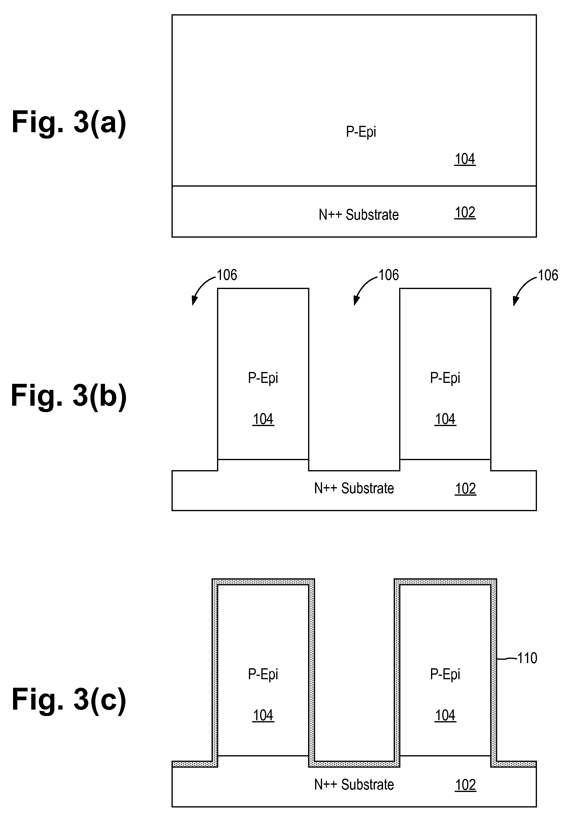
[0052]NMOS transistor 100 is formed on a very heavily doped N++ substrate 102. N++ substrate 102 serves as the drain electrode of the transistor. Oxide-filled trenches 112 are formed in a P-type epitaxial (P-Mesa-Epi) lay...

second embodiment

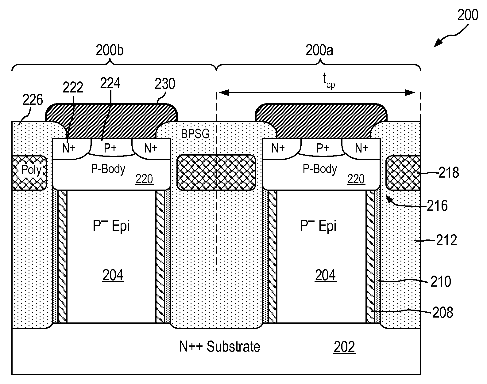
[0066]FIG. 2 is a cross-sectional view of a vertical trench MOSFET device according to the present invention. Referring to FIG. 2, an N-type vertical trench MOSFET device (“NMOS transistor”) 200 is formed in an array of parallely connected transistor cells 200a and 200b. A desired number of transistor cells are used to form the array to realize an NMOS transistor 200 having the desired breakdown voltage characteristic. The transistor array can be a 1-dimensional or 2-dimensional array depending on the number of transistor cells involved.

[0067]NMOS transistor 200 has the same structure as NMOS transistor 100 of FIG. 1 except for an additional thin P-type epitaxial (P-Epi) layer 208 formed adjacent to the thin N-Epi layer 210. The N-Epi layer 210 and P-Epi layer 208 forming a “double nanotube” structure. Furthermore, the P-type epitaxial layer 204 in which the transistor cells are formed is very lightly doped P-type epitaxial layer, denoted “P-Mesa Epi” in FIG. 2. The thin P-Epi layer...


PUM


Abstract

A method for forming a semiconductor device includes forming a nanotube region using a thin epitaxial layer formed on the sidewall of a trench in the semiconductor body. The thin epitaxial layer has uniform doping concentration. In another embodiment, a first thin epitaxial layer of the same conductivity type as the semiconductor body is formed on the sidewall of a trench in the semiconductor body and a second thin epitaxial layer of the opposite conductivity type is formed on the first epitaxial layer. The first and second epitaxial layers have uniform doping concentration. The thickness and doping concentrations of the first and second epitaxial layers and the semiconductor body are selected to achieve charge balance. In one embodiment, the semiconductor body is a lightly doped P-type substrate. A vertical trench MOSFET, an IGBT, a Schottky diode and a P-N junction diode can be formed using the same N-Epi / P-Epi nanotube structure.

Description

CROSS-REFERENCE TO RELATED APPLICATION[0001]The present application is related to concurrently filed and commonly assigned U.S. patent application entitled “Nanotube Semiconductor Devices,” of the same inventors hereof, having patent application Ser. No. 12 / 484,170, which patent application is incorporated herein by reference in its entirety.FIELD OF THE INVENTION[0002]The invention relates to nanotube vertical trench MOSFET semiconductor devices and, in particular, to a process of forming nanotube vertical trench MOSFET devices using sidewall epitaxial layers. Furthermore, the invention relates to structures for edge termination in charge balance power devices.DESCRIPTION OF THE RELATED ART[0003]Metal-oxide-silicon field effect transistor (MOSFET) devices are formed using various lateral and vertical structures. Lateral MOSFET devices have fast switching speed but are less dense than vertical MOSFET devices. Vertical MOSFET devices can be used to form a high density array of transi...

Claims


Application Information

Patent Timeline
Patent Type & Authority Patents(United States)
IPC IPC(8): H01L21/311
CPCB82Y10/00H01L29/0665H01L29/0692H01L29/1095H01L29/6609H01L29/66143H01L29/66348H01L29/66666H01L29/7397H01L29/861H01L29/872H01L29/7813H01L29/66734H01L29/0634
Inventor YILMAZ, HAMZAWANG, XIAOBINBHALLA, ANUPCHEN, JOHNCHANG, HONG
Owner ALPHA & OMEGA SEMICON INC
Why Eureka
Try Eureka