High switching trench mosfet

a high-switching, trench technology, applied in the direction of semiconductor devices, basic electric elements, electrical apparatus, etc., can solve the problems of difficulty in cell pitch shrinkage, additional cost for the implementation of resistive elements b>101/b>, etc., to enhance the performance of shielded gate trench mosfet and cos

Active Publication Date: 2012-11-22
FORCE MOS TECH CO LTD
View PDF1 Cites 47 Cited by
  • Summary
  • Abstract
  • Description
  • Claims
  • Application Information

AI Technical Summary

Benefits of technology

[0008]By providing a power semiconductor device, for example a shielded gate trench MOSFET according to the present invention, the shielded electrode spreading resistance replaces the resistive element in the prior art by a...

Problems solved by technology

However, according to the prior art, the resistive element 101 is implemented by poly-silicon, diffusion or other suitable material as long as the resistive element 101 is greater than overall distribution or spreading resistance of the shielded electrode 102, therefore,...

Method used


Image

  • High switching trench mosfet
  • High switching trench mosfet
  • High switching trench mosfet

Examples


Embodiment Construction

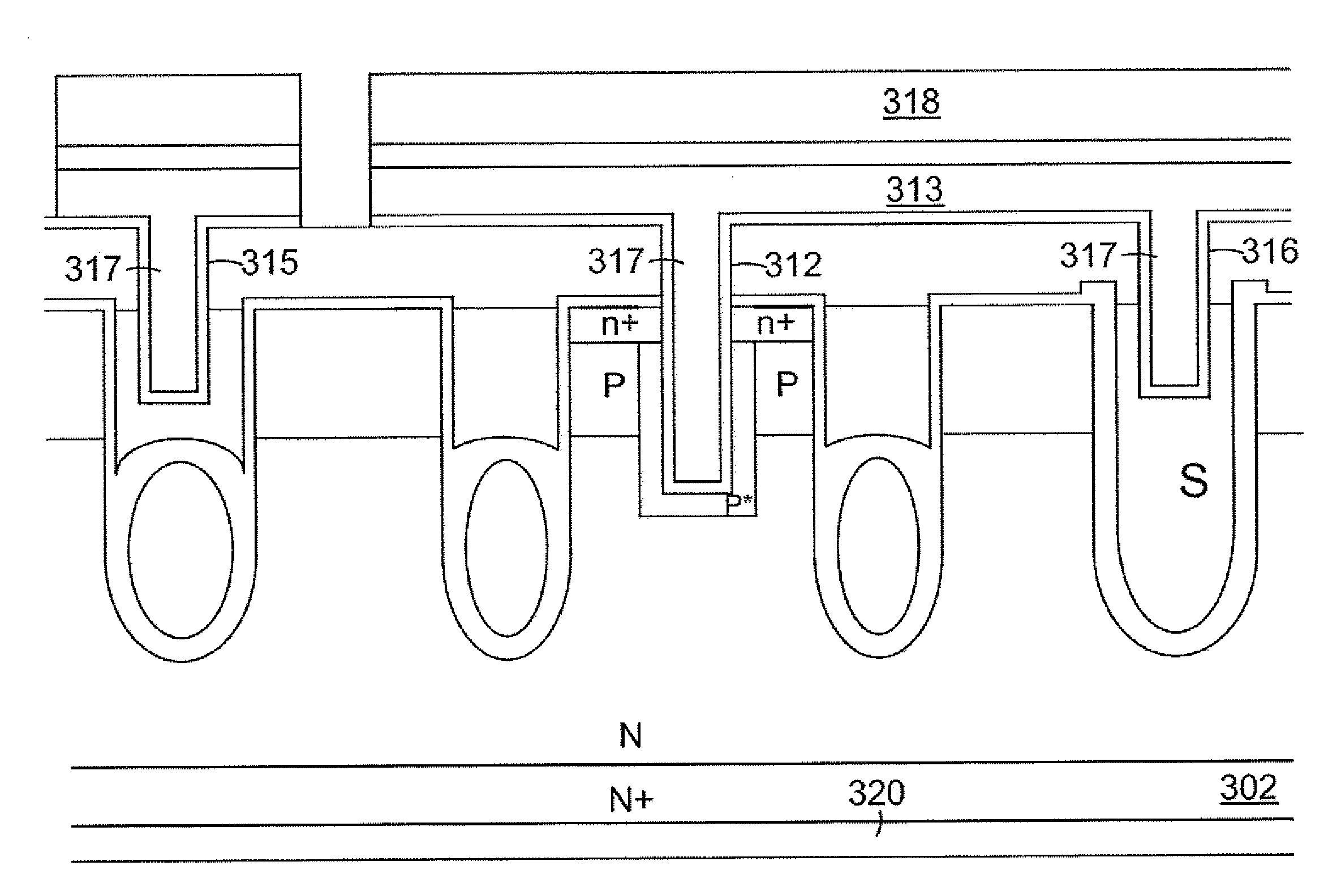
[0025]FIG. 2 is a cross-sectional view showing a shielded gate trench MOSFET 200 according to a preferred embodiment of the present invention. The shielded gate trench MOSFET 200 is formed in a silicon layer, for example an epitaxial layer 201 of a first conductivity type, here n-type, grown on top surface of an N+ semiconductor substrate 202 having same conductivity type with the N epitaxial layer 201 and padded by a back metal on rear side as drain metal 220. A plurality of gate trenches 203 in active area, at least one gate trench 203′ and 203″ in gate electrode contact area, and at least one gate trench 203″ in shielded electrode contact area are extending from top surface of the N epitaxial layer 201 to a certain depth. Among those gate trenches, the gate trench 203′ in the gate electrode contact area and the gate trench 203″ in the shielded electrode contact area each has greater trench width than the gate trenches 203 in the active area for wider electrode contact. The gate t...


PUM


Abstract

A shielded gate trench metal oxide semiconductor filed effect transistor (MOSFET) having high switching speed is disclosed. The inventive shielded gate trench MOSFET includes a shielded electrode spreading resistance placed between a shielded gate electrode and a source metal to enhance the performance of the shielded gate trench MOSFET by adjusting doping concentration of poly-silicon in gate trenches to a target value. Furthermore, high cell density is achieved by employing the inventive shielded gate trench MOSFET without requirement of additional cost.

Description

FIELD OF THE INVENTION[0001]This invention relates in general to semiconductor devices, and more particularly, to an improved and novel device configuration for providing a metal oxide semiconductor field effect transistor (MOSFET) with high switching speed.BACKGROUND OF THE INVENTION[0002]Compared to a conventional trench metal oxide semiconductor field effect transistor (hereinafter MOSFET), a shielded gate trench MOSFET is more attractive due to its reduced Cgd (capacitance between gate and drain) in accordance with reduced Qgd (charge between gate and drain), and increased breakdown voltage of the trench MOSFET, making an excellent choice for power switching applications such as inverter and DC to DC power supply circuits. However, for those power switching applications, MOSFET body diode reverse recovery charge is very important due to the fact that high body diode reverse recovery charge value increase complimentary MOSFET turn-on loss, which pronounces especially when the shi...

Claims


Application Information

Patent Timeline
IPC IPC(8): H01L29/78H01L21/336
CPCH01L29/0865H01L29/1095H01L29/407H01L29/41741H01L29/41766H01L29/7813H01L29/4238H01L29/456H01L29/66727H01L29/66734H01L29/7811H01L29/4236
Inventor HSIEH, FU-YUAN
Owner FORCE MOS TECH CO LTD
Why Eureka
Try Eureka