Apparatus for manufacturing printed wiring board and method for manufacturing printed wiring board using the same

a manufacturing apparatus and printed wiring technology, applied in the direction of lighting and heating apparatus, mechanical control devices, instruments, etc., can solve the problems of difficult to precisely and uniformly etch copper on both upper and lower surfaces, the difference between the upper and lower surfaces is likely to be much greater, and the etching speed is likely to differ substantially between the upper and lower surfaces of printed wiring boards, so as to reduce productivity or hike, the effect of uniform etching speed and high precision

Inactive Publication Date: 2005-07-19
PANASONIC CORP
View PDF18 Cites 14 Cited by
  • Summary
  • Abstract
  • Description
  • Claims
  • Application Information

AI Technical Summary

Benefits of technology

[0018]In this apparatus, since the nozzle pipes are disposed at narrower intervals at central positions on the upper surface, in order that the etchant may flow down immediately without staying in the center of the upper surface by increasing the amount of the etchant sprayed to the center on the printed wiring board, the pressure of the central nozzle pipe may be set higher than the pressure of the nozzle pipes at both sides easily by controlling the opening degree of the pressure regulating valves while observing the indication of the pressure gauges.
[0019]Accordingly, the etching speed is made uniform in the central area and peripheral area and on the upper surface and lower surface, and a conductor pattern of high precision is formed, so that a simple etching apparatus of a printed wiring board is presented without lowering the productivity or hiking the apparatus manufacturing cost.

Problems solved by technology

In such conventional etching apparatus and etching method, it is difficult to etch the copper precisely and uniformly on both upper and lower surfaces, and in particular the etching speed is likely to differ substantially between the upper surface and lower surface of the printed wiring board.
As a result, a significant difference occurs in the etching precision of conductor pattern between the central area and peripheral area of the upper surface of the printed wiring board, and the difference is much greater between the upper surface and lower surface, and it is extremely difficult to etch the conductor pattern of printed wiring board of high density and high precision, and the process yield is extremely lowered, and this problem is more notable when the thickness of the printed wiring board is smaller and the density of the conductor pattern is higher.
To solve these problems, hitherto, it has been attempted to incline the printed wiring board or set upright, and inject the etchant from the spray nozzles in the horizontal direction, and various methods for eliminating retention of etchant have been proposed, but it is difficult to convey the printed wiring board and set the etching condition, and the productivity is significantly impaired, and the manufacturing cost of the manufacturing apparatus is soaring, and it is not widely employed at the present.

Method used


Image

  • Apparatus for manufacturing printed wiring board and method for manufacturing printed wiring board using the same
  • Apparatus for manufacturing printed wiring board and method for manufacturing printed wiring board using the same
  • Apparatus for manufacturing printed wiring board and method for manufacturing printed wiring board using the same

Examples


embodiment 1

(Embodiment 1)

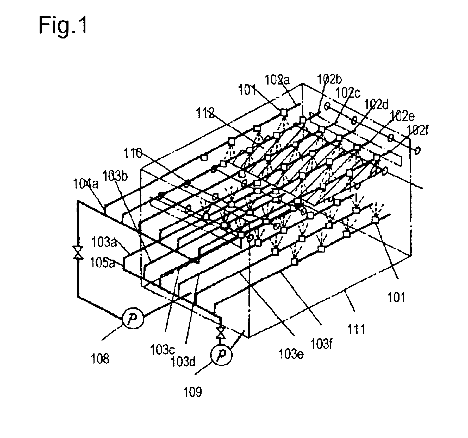
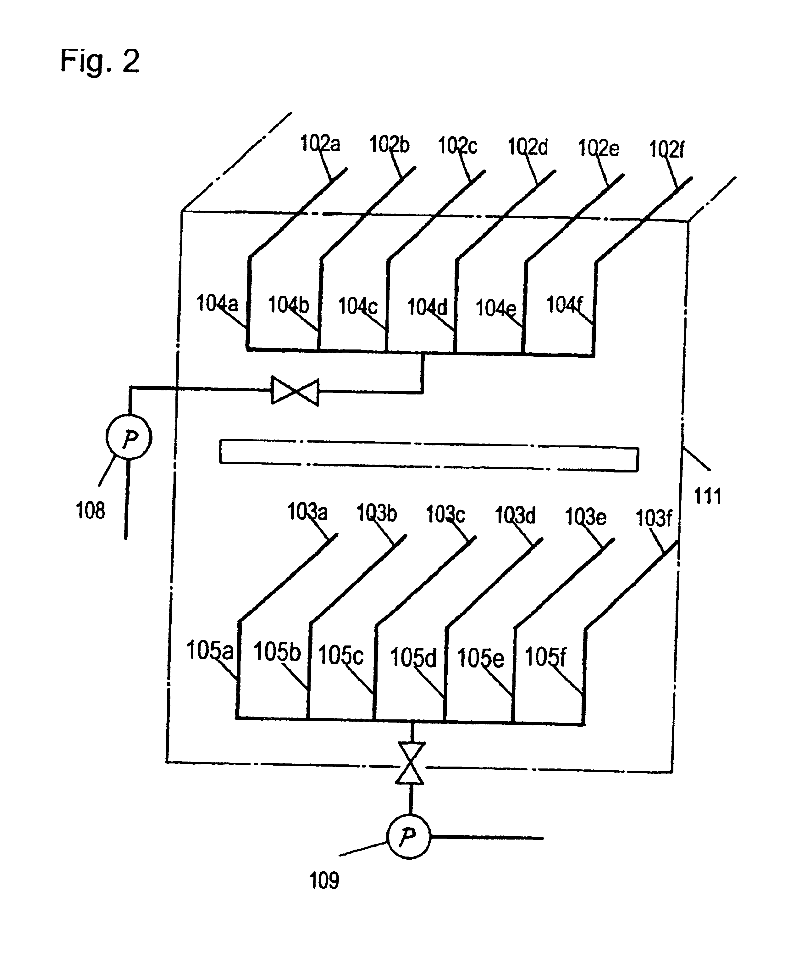
[0055]Embodiment 1 of the invention is described by referring to the accompanying drawings. FIG. 1 shows an outline of a manufacturing apparatus of printed wiring board in embodiment 1 of the invention, and FIG. 2 is a schematic diagram showing the detail of the manufacturing apparatus in embodiment 1 of the invention.

[0056]In FIG. 1, plural upper surface nozzle pipes 102a to 102f disposed nearly at equal intervals in an etching booth 111 are individually provided with a plurality of spray nozzles 101, and are disposed parallel to or at a certain angle to the running direction of the printed wiring board. Similarly, plural lower surface nozzle pipes 103a to 103f disposed nearly at equal intervals in the etching booth 111 are individually provided with a plurality of spray nozzles 101, and are disposed parallel to or at a certain angle to the running direction of the printed wiring board. An upper surface spray pump 108 supplies an etchant to the nozzle pipes 102a to 10...

embodiment 2

(Embodiment 2)

[0067]Embodiment 2 of the invention is described by referring to the accompanying drawings. FIG. 3 is an outline diagram of a manufacturing apparatus of printed wiring board in embodiment 2 of the invention, and FIG. 4 is a detailed diagram of the manufacturing apparatus of printed wiring board in embodiment 2 of the invention.

[0068]In FIG. 3, plural upper surface nozzle pipes 202a to 202e disposed in an etching booth 211 are individually provided with a plurality of spray nozzles 201, and are disposed parallel to or at a certain angle to the running direction of the printed wiring board. Similarly, plural lower surface nozzle pipes 203a to 203e are individually provided with a plurality of spray nozzles 201, and are disposed parallel to or at a certain angle to the running direction of the printed wiring board. An upper surface spray pump 208 supplies an etchant to the nozzle pipes 202a to 202e through upper surface pressure regulating valves 206a to 206e as means for...

embodiment 3

(Embodiment 3)

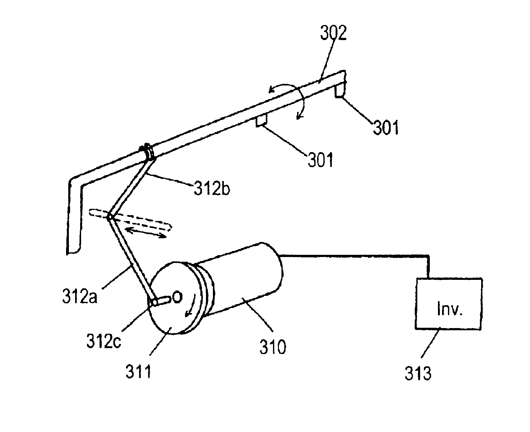
[0088]Embodiment 3 of the invention is described by referring to the accompanying drawings. FIG. 5 and FIG. 6 are outline diagrams of an etching apparatus as a manufacturing apparatus of printed wiring board in embodiment 3 of the invention, and FIG. 7 is a detailed diagram of an oscillating mechanism of nozzle pipes of the manufacturing apparatus in the embodiment of the invention.

[0089]An etching apparatus is explained as the manufacturing apparatus of printed wiring board in embodiment 3 of the invention.

[0090]The configuration of the etching apparatus in embodiment 3 of the invention is similar to a conventional apparatus for etching from both upper surface and lower surface simultaneously, and the upper structure and lower structure are basically the same. For the ease of explanation of the invention, therefore, only the upper structure is explained by referring to the drawings.

[0091]As shown in FIG. 5, upper surface nozzle pipes 302a to 302f are disposed parallel...


PUM

PropertyMeasurementUnit
angleaaaaaaaaaa
thicknessaaaaaaaaaa
widthaaaaaaaaaa

Abstract

In a manufacturing apparatus of printed wiring board an aperture of a nozzle pipe located in a central position is larger than that at both sides, or the aperture of the piping to the nozzle pipe in the central position is larger than that of the piping at both sides. The mutual interval is narrower with the central nozzle pipes. The interval of the individual nozzle pipes is variable, and is also variable in the vertical direction. A pressure-proof flexible tube is provided between each nozzle pipe and the pump, and the interval of the individual nozzle pipes is variable, and is also variable in the vertical direction. Further, the spray pressure, oscillating angle, and oscillating speed can be set individually in each nozzle pipe, and such setting can be automated.

Description

DESCRIPTION[0001]Manufacturing apparatus of printed wiring board, and manufacturing method of printed wiring board using the sameTECHNICAL FIELD[0002]The present invention relates to a manufacturing apparatus of printed wiring board used in various electronic appliances.BACKGROUND ART[0003]Recently, as the electronic appliances are becoming smaller in size and diversified in function, printed wiring boards widely used in such electronic appliances are required to be higher in wiring density and higher in reliability.[0004]A conventional manufacturing apparatus used in forming conductor patterns in printed wiring boards, especially an etching apparatus is explained.[0005]FIG. 21 is a schematic view of a conventional etching apparatus as a manufacturing apparatus of printed wiring boards. In FIG. 21, plural upper surface nozzle pipes 632 and plural lower surface nozzle pipes 633 disposed in an etching booth 641 are respectively provided with a plurality of spray nozzles 631.[0006]An u...

Claims


Application Information

Patent Timeline
Patent Type & Authority Patents(United States)
IPC IPC(8): C23F1/08H05K3/06
CPCC23F1/08H05K3/068
Inventor HIGA, KAZUTOMO
Owner PANASONIC CORP
Why Eureka
Try Eureka