High impedance structures for multifrequency antennas and waveguides

Inactive Publication Date: 2005-07-19
TELEDYNE SCI & IMAGING
8 Cites 29 Cited by

AI-Extracted Technical Summary

Problems solved by technology

The structure also suppresses current and substrate modes, reducing the ...

Method used

[0052]Also, the gaps between the patches prevent surface current at each layer. This along with the L-C circuits presented by the layers help suppress surface and substrate modes and increase the front-to-back ratio, thereby improving the antenna signal.
[0057]As shown in FIG. 11b, the amplifier section 102 of the waveguide contains a square waveguide 108 with the layered structure mounted on all four walls 109a-109d to support both a signal that is horizontally and vertically (cross polarized). Amplifier arrays 104 (see FIG. 10) are generally transmission devices rather than a reflection devices, with the signal entering one side of the array amplifier and the amplified signal transmitted out the opposite side. During transmission, amplifiers arrays also change polarity of the signal which reduces spurious oscillations. However, a portion of the input signal will maintain its input polarization as it transits the amplifier array. In addition, a portion of the output signal will reflect back...

Benefits of technology

[0020]The new structure is particularly applicable to microstrip patch and slot antennas, and to waveguides. In patch antennas, the invention provides an efficient adaptive reflective backplane over a greater range of frequencies than has previously been attainable. The layered structure can be designed to adapt its reflected phase to maintain an optimum electrical distance over multiple frequencies. The structure also suppresses current and substrate modes, reducing the degradation of the antenna's performance due to these undesired effects. The gaps between the patches reduce the undesired effects produced by surface current.
[0021]For waveguides that transmit a signal in one polarity (vertical or horizontal), the new wall structure is used for two opposing walls. For waveguides that transmit cross-polarized signals (both horizontal...

Abstract

A multi layered high impedance structure presents a high impedance to multiple frequency signals, with a different frequency for each layer. Each layer comprises a dielectric substrate, and an array of radiating elements such as parallel conductive strips or conductive patches on the substrate's top surface, with a conductive layer on the bottom surface of the bottommost layer. The radiating elements of succeeding layers are vertically aligned with conductive vias extending through the substrates to connect the radiating elements to the ground plane. Each layer presents as a series of parallel resonant L-C circuits to an E field at a particular signal frequency, resulting in a high impedance surface at that frequency. The new structure can be used as the substrate for a microstrip patch antenna to provide an optimal electrical distance between the resonator and backplane at multiple frequencies. It can also be used in waveguides that transmit multiple signal frequencies signals in one polarization or that are cross-polarized. As a waveguide it maintains a near-uniform density E and H fields, resulting in near uniform signal power density across the waveguide's cross-section.

Application Domain

Technology Topic

PhysicsElectrical distance +11

Image

  • High impedance structures for multifrequency antennas and waveguides
  • High impedance structures for multifrequency antennas and waveguides
  • High impedance structures for multifrequency antennas and waveguides

Examples

  • Experimental program(1)

Example

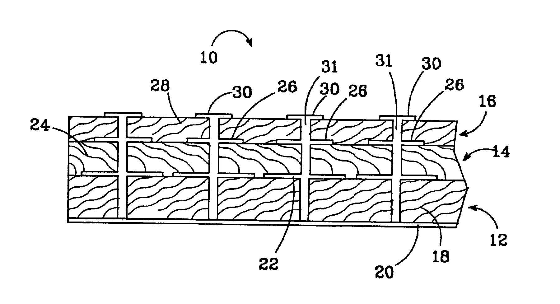
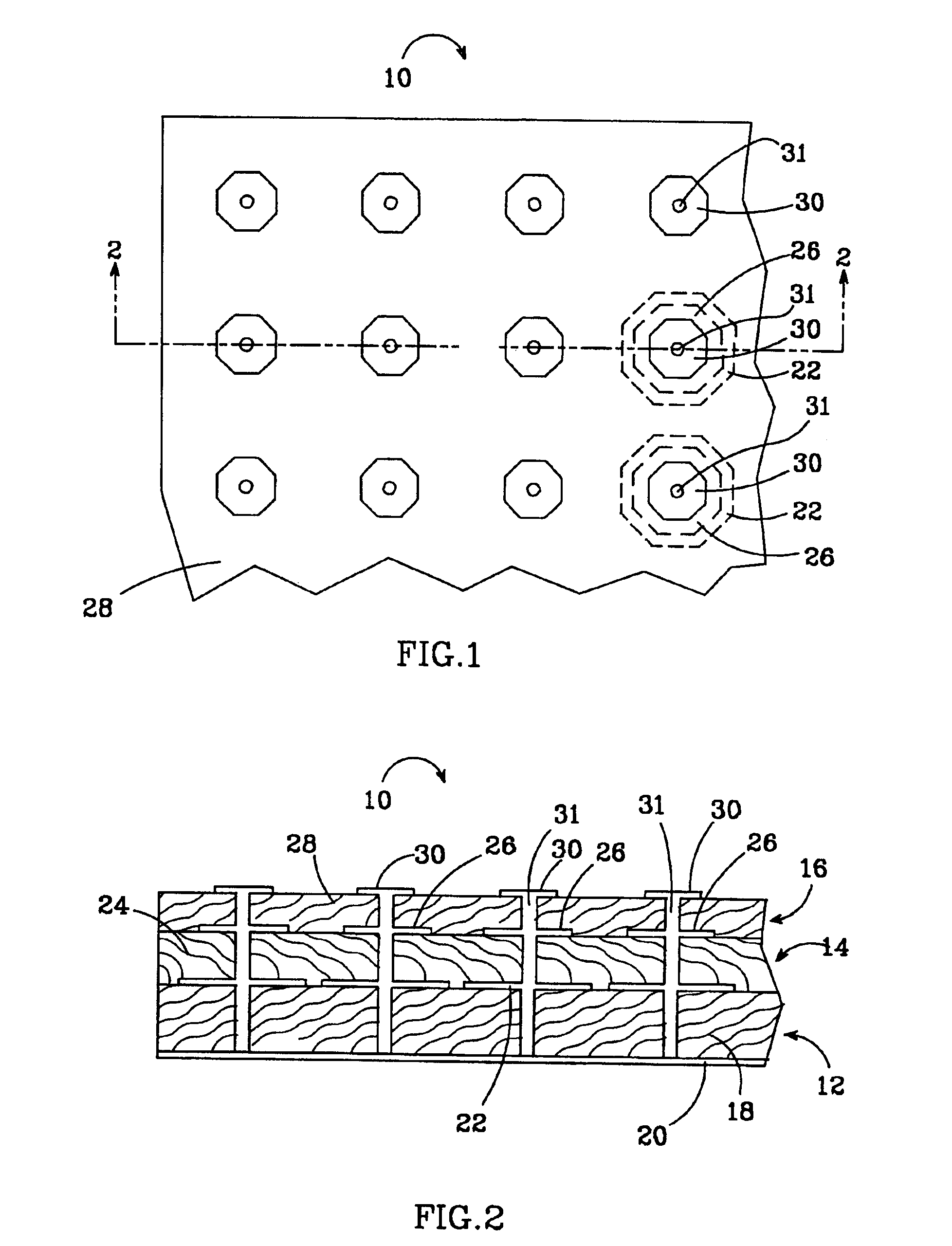
[0034]FIGS. 1 and 2 show one embodiment of a new layered high impedance structure 10 in which conductive hexagonal patches are provided on each layer. The new structure can have different numbers of layers, depending upon the number of different signal frequencies to be transmitted. Referring to FIG. 2, the embodiment shown has three similar layers 12, 14, and 16, with each layer having different dimensions or made from different materials such that each presents as a high impedance to the E field from a different respective signal frequency bandwidth.
[0035]As further shown in FIG. 2, the bottom layer 12 comprises a substrate of dielectric material 18 with an array of preferably equally spaced conductive patches 22 on its upper surface (see also FIG. 1). The bottom layer also has a conductive layer 20 on its bottom surface. The second layer 14 does not have a conductive layer, but is otherwise similar to and formed over the bottom layer 12 with conductive patches 26 (see also FIG. 1) located directly above and vertically aligned with the first layer patches 22. The second layer's dielectric substrate 24 is thinner than the first layer's substrate 18 and its patches 26 are smaller than the first layer's patches 22. The distance between adjacent patches 26 is greater than the distance between patches 22. These differences cause the second layer to present a high impedance as a frequency bandwidth greater than for the first layer.
[0036]The third layer 16 is similar to the second layer 14. Its dielectric substrate 28 is thinner than substrates 18 and 24, and it's patches 30 (see also FIG. 1) are located directly above and vertically aligned with patches 22 and 26. The patches 30 are smaller than the patches below it and the distance between adjacent patches is greater.
[0037]Conductive vias 31 extend through each of the dielectric substrates 18, 24 and 28, to connect the vertically aligned patches of each layer to the conductive layer 20. The vias 31 can have different cross-sections such as square or circular.
[0038]FIGS. 3 and 4 show another three-layered embodiment of the invention with parallel conductive strips instead of conductive patches. It also presents a high impedance to E fields at three different frequency bandwidths, but the E fields must have a component that is transverse to the conductive strips. Like the patch embodiment 10, each of its layers 32, 34, and 36 (shown in FIG. 4) have respective dielectric substrates 38, 40, and 42 that are progressively thinner from the bottom layer 32 to the top 36. Conductive strips 44, 46, and 48 are provided respectively on substrates 32,34 and 36 and are progressively thinner from the bottom layer to the top. The strips in each layer are parallel and aligned over the strips in the layers below and above, and preferably have uniform width and a uniform gap between adjacent strips. Because the width of the strips progressively decreases for each successive layer, the gaps between adjacent strips progressively increases.
[0039]The new structure 40 also includes vias 50 that connect each vertically aligned set of strips to a ground plane conductive layer 52 (see FIG. 2) located at the underside of the bottom layer 32. The vias are preferable equally spaced down the longitudinal centerlines of the strips. The location of the vias 50 can be staggered for adjacent strips.
[0040]The new structure is constructed by stacking layers of metalized dielectric substrates. Numerous materials can be used for the dielectric substrates, including but not limited to plastics, poly-vinyl carbonate (PVC), ceramics, or high resistance semiconductor materials such as Gallium Arsenide (GaAs), all of which are commercially available. Each layer in the new structure can have a dielectric substrate of a different material and/or a different dielectric constant. A highly conductive material such as copper or gold (or a combination thereof) should be used for the conductive layer, patches, strips, and vias.
[0041]In the strip embodiment, parallel gaps in the conductive material are then etched away using any of a number of etching processes such as acid etching or ion mill etching. Within each layer, the etched gaps are preferably of the same width and the same distance apart, resulting in parallel conductive strips on the dielectric substrate of uniform width and with uniform gaps between adjacent strips. In the case of the patch embodiment, the conductive material can be etched away by the same process, preferably leaving equally spaced and equally shaped patches of conductive material. A preferred shape for the patches is hexagonal, but other shapes can also be used.
[0042]The different layers are then stacked with the strips or patches for each layer aligned with corresponding ones in the layers above and below. The layers are bonded together using any of the industry standard practices commonly used for electronic package and flip-chip assembly. Such techniques include solder bumps, thermo-sonic bonding, electrically conductive adhesives, and the like.
[0043]Once the layers are stacked, holes are formed through the structure for the vias. The holes can be created by various methods, such as conventional wet or dry etching. The holes are then filled or at least lined with the conductive material and preferably at the same time, the exposed surface of the bottom substrate is covered with a conductive material to form conductive layers 20 or 52. A preferred processes for this is sputtered vaporization plating. The holes do not need to be completely filled, but the walls must be covered with the conductive material sufficiently to eclectically connect the ground plane to the radiating elements of each layer.
[0044]Each layer in the structure presents a pattern of parallel resonant L-C circuits and a high impedance to an E field for different signal frequencies. The bottom most layer presents a high impedance to the lowest frequency and the top most layer presents as a high impedance to the highest frequency. For the strip embodiment, at least a component of, and preferably the entire E field, must be transverse to the strips. A signal normally incident on this structure and within one of the frequency bandwidths, will ideally be reflected with a reflection coefficient of +1 at the resonant frequency, as opposed to a −1 for a conductive material.
[0045]The capacitance of each layer is primarily dependant upon the widths of the gaps between adjacent strips or patches, but is also impacted by the dielectric constants of the respective dielectric substrates. The inductance is primarily dependent upon the substrate thickness and the diameter of the vias.
[0046]The dimensions and/or compositions of the various layers are different to produce the desired high impedance to different frequencies. To resonate at higher frequencies, the thickness of the dielectric substrate can be decreased, or the gaps between the conductive strips or patches can be increased. Conversely, to resonate at lower frequencies, the thickness of the substrate can be increased or the gaps between the conductive strips or patches can be decreased. Another contributing factor is the dielectric constant of the substrate, with a higher dielectric constant increasing the gap capacitance. These parameters dictate the dimensions of the structures 30 and 40. Accordingly, the layered high impedance ground plane structures described herein are not intended to limit the invention to any particular structure or composition.
[0047]For example, in a two layer patch embodiment presenting high impedances to the E-fields of 22 GHz and 31 GHz signals and having substrates with a 3.27 dielectric constant, the top and bottom substrates are 30 mils and 60 mils thick, respectively. The patches are hexagonal with a center-to-center spacing of 62.2 mil. The patches on each layer are the same size and the gap between adjacent patches is 10 mil. The vias have a square 15 mil by 15 mil cross section and extend through both layers. The patches are centered on the vias in both layers.
[0048]The layers of the new wall structure also act as a high impedance to a limited frequency band around their design frequency, usually within a 10-15% bandwidth. For example, a layer in the structure designed for a 35 GHz signal will present a high impedance to a frequency range of about 32.5-37.5 GHz. As the frequency deviates from the design resonant frequency, the performance of the surface structure degrades. For frequencies far above the center frequency, the patches or strips will simply appear as conductive sheets. For frequencies far below the design frequency, the layer will be transparent.
[0049]FIG. 5 illustrates the network of capacitance and inductance presented by a new three layer structure which produces an array of resonant L-C circuits to three progressively higher frequencies f1, f2 and f3. The bottommost layer appears as a high impedance surface to signal f1 as a result of a series of resonant L-C L1/C1 representing the equivalent inductance and capacitance presented by the bottommost layer to its design frequency bandwidth. The second and third layers also for respective series of resonant L-C circuits L2/C2 and L3/C3, at their frequency bandwidths.
[0050]FIGS. 6a-6c illustrate how the three signals interact with layers of the new structure 60, for both the conductive patch and conductive strip embodiments. An important characteristic of the structure's layers 62, 64, and 66 is that each appears transparent to E fields at frequencies below its design frequency, while the strips or patches in each appear as a conductive surface to E fields at frequencies above its design frequency. For the highest frequency signal f3, the top layer 66 will present high impedance resonant L-C circuits to the signal's E field. The patches/strips 68 (see FIG. 6a) on second layer 64 appear as a conductive layer and become a “virtual ground” for the top layer 62. f2 (see FIG. 6b) is lower in frequency than f1 (see FIG. 6a) and, as a result, the first layer 62 will be transparent to f2's E field, while the second layer 64 will appear as high impedance resonant L-C circuits. The patches 70 (see FIG. 6c) on the third layer will appear as a conductive layer, becoming the second layer's virtual ground. Similarly, at f3 (see FIG. 6c) the top and second layers 62 and 64 will be transparent, but the third layer 66 will appear as high impedance resonant L-C circuits, with the conductive layer 72 (see FIG. 6c) operating for the third layer 66.
[0051]FIG. 7 shows a microstrip antenna 80 using the new layered high impedance structure 82 as its backplane. In the preferred embodiment, the structure has hexagonal patches 84 instead of strips. Conventional microstrip antennas transmit at only one frequency, depending upon the thickness of the dielectric layer. Using the new structure, a microstrip antenna can transmit at multiple frequencies. An optimal electrical distance is maintained between the emitting element and the respective ground (virtual or actual) for each of the transmission frequencies. At the highest frequency, the antenna signal sees only the L-C circuits of the structures top layer 85, and the virtual ground provided by the second layer 86 will provide the optimal electrical distance. For the next highest frequency, the signal sees only the L-C circuits of the second layer 86 and the virtual ground of the bottom layer 87 provides the optimal electrical distance. For the lowest frequency at which the bottom layer 87 responds, the conductive layer 88 provides the optimal electrical distance.
[0052]Also, the gaps between the patches prevent surface current at each layer. This along with the L-C circuits presented by the layers help suppress surface and substrate modes and increase the front-to-back ratio, thereby improving the antenna signal.
[0053]The new groundplane structure with conductive strips can also be used as the sidewalls of a waveguide or mounted to a waveguide's sidewalls by a variety of adhesives such as silicon glue. FIG. 8 shows a new metal waveguide 90 having the new layered structure mounted on the interior of all four walls 92a-d, with the conductive strips 93 oriented inward and longitudinally down the waveguide. The layered wall structure allows the waveguide 90 to transmit signals at multiple frequencies with both horizontal and vertical polarizations, while maintaining a uniform power density. The vertically polarized signal has a vertical E field component and a horizontal H field component. The E field maintains a uniform density as a result of the high impedance presented by the wall structure on the vertical sidewalls 92a and 92c. Current will also flow down the strips 93 on the top wall 92b and/or bottom wall 92d, maintaining a uniform H field. For the horizontally polarized signal, the E field will maintain a generally uniform power density because of the layered structure at the top and bottom wall 92b and 92d, and the H field will remain uniform because of current flowing down the conductive strips 93 of the sidewalls 92a and 92c. Thus, the cross-polarized signal will have a generally uniform power density across the waveguide. If the waveguide is transmitting a signal in one polarization (vertical or horizontal), it only needs the new layered structure on only two opposing walls to maintain the signals uniform power density: sidewalls for vertical polarization, and top and bottom for horizontal.
[0054]FIGS. 9, 10 and 11a-c show a metal waveguide 100 with the new layered high impedance wall structure used on two walls in certain sections of the waveguide (FIGS. 11a and 11b) and on all four walls in another section (FIG. 11c). The new waveguide 100 can transmit signals with a uniform power density at different frequencies, the number of frequencies depending upon the number of layers in the wall structure. Referring to FIGS. 9 and 10, the waveguide comprises a horn input section 101, an amplifier section 102, and a horn output section 103. An amplifier array 104 is mounted in the amplifier section 102, near the middle.
[0055]The amplifier array 104 has a larger area than the cross section of the standard sized high frequency metal waveguide. As a result, the cross section of the signal must be increased from the standard size waveguide to accommodate the area of amplifier array 104 such that all amplifier elements of the array will experience the transmission signal. As shown in FIG. 10, the input section 101 has a tapered horn guide 105 that enlarges the beam to accommodate the larger amplifier array 104, while maintaining a single mode signal.
[0056]An input signal with vertical polarization enters the waveguide at the input adapter 106. As shown in FIG. 11a a new surface structure similar to the one shown in FIGS. 3 and 4 is affixed to the vertical sidewalls 107a and 107b of the input section 101. The polarization of the signal remains vertical throughout the input section 101. The E field component of the signals in the input section 101 will have a vertical orientation, with the H field component perpendicular to the E field. In this orientation, the new wall structure on sidewalls 107a and 107b will appear as an open circuit to the transverse E field, providing a hardwall boundary condition. In addition, current will flow down the top and/or bottom conductive wall, providing for a uniform H field. The uniform E and H fields provide for a near uniform signal power density across the input section 101.
[0057]As shown in FIG. 11b, the amplifier section 102 of the waveguide contains a square waveguide 108 with the layered structure mounted on all four walls 109a-109d to support both a signal that is horizontally and vertically (cross polarized). Amplifier arrays 104 (see FIG. 10) are generally transmission devices rather than a reflection devices, with the signal entering one side of the array amplifier and the amplified signal transmitted out the opposite side. During transmission, amplifiers arrays also change polarity of the signal which reduces spurious oscillations. However, a portion of the input signal will maintain its input polarization as it transits the amplifier array. In addition, a portion of the output signal will reflect back to the to the waveguide area before the amplifier. Thus, in amplifier section 102 (see FIG. 11b) a signal with vertical and horizontal polarizations can exist.
[0058]As described above, the strip embodiment of the new wall structure allows the amplifier section 102 to support a signal with both vertical and horizontal polarizations. The wall structure presents a high impedance to the transverse E field of both polarizations, maintaining the E field density across the waveguide for both. The strips allow current to flow down the waveguide in both polarizations, maintaining a uniform H field density across the waveguide for both. Thus, the cross polarized signal will have uniform density across the waveguide.
[0059]Matching grid polarizers 111 and 112 (see FIG. 10) are mounted on each side of and parallel to the array amplifier 104, parallel to the array amplifier. The polarizers appear transparent to one signal polarization while reflecting a signal with an orthogonal polarization. For example, the output grid polarizer 112 allows a signal with an output polarization to pass, while reflecting any signal with an input polarization. The input polarizer 111 allows a signal with an input polarization to pass, while reflecting any signal with an output polarization. The distance of the polarizers from the amplifier can be adjusted, allowing the polarizers to function as input and output tuners for the amplifier, that provide a maximum benefit at a specific distance from the amplifier.
[0060]The output grid polarizer 112 reflects any input signal transmitted through the array amplifier 104 with a horizontal polarization. Thus, the signal at the output section 103 (see FIGS. 10 and 11c) will have only a vertical output polarity. Like the input section 101, the output section 103 is also a tapered horn guide 113 but is used to reduce the cross section of the amplified signal for transmission in a standard high frequency waveguide. As shown in FIG. 11c, to maintain a uniform density signal in the output section, the layered structures are mounted on the top and bottom walls 114a and 114b of the output section, with the strips oriented longitudinally down the waveguide. This allows for the output signal to maintain a near uniform power density. The output adapter 116 transmits the amplified signal out of the waveguide.
[0061]Although the present invention has been described in considerable detail with reference to certain preferred configurations thereof, other versions are possible. The surface structure described can be used in applications other than antennas and waveguides. It can be used in other applications needing a high impedance surface to the E field component of signals at different frequencies. Therefore, the spirit and scope of the appended claims should not be limited to the preferred versions described in the specification.

PUM

no PUM

Description & Claims & Application Information

We can also present the details of the Description, Claims and Application information to help users get a comprehensive understanding of the technical details of the patent, such as background art, summary of invention, brief description of drawings, description of embodiments, and other original content. On the other hand, users can also determine the specific scope of protection of the technology through the list of claims; as well as understand the changes in the life cycle of the technology with the presentation of the patent timeline. Login to view more.

Similar technology patents

Classification and recommendation of technical efficacy words

Why Eureka
Try Eureka