Method for making a socket to perform testing on integrated circuits

a technology for integrated circuits and sockets, applied in the direction of semiconductor/solid-state device testing/measurement, coupling device connections, instruments, etc., can solve the problems of unreliable pogo pins, unreliable pogo pins, and limited sockets in conventional sockets

Inactive Publication Date: 2005-07-26
FORMFACTOR INC
View PDF8 Cites 71 Cited by
  • Summary
  • Abstract
  • Description
  • Claims
  • Application Information

AI Technical Summary

Problems solved by technology

Unfortunately, limitations exists in conventional sockets.
Conventional sockets maybe expensive to manufacture and somewhat unreliable.
Such pogo pins are unreliable and non-wiping.
Pogo pins also limit the pitch of an interconnect structure in a socket.
For example, a pitch of less than 40 mils with pogo pins becomes mechanically difficult and prohibitively expensive.

Method used


Image

  • Method for making a socket to perform testing on integrated circuits
  • Method for making a socket to perform testing on integrated circuits
  • Method for making a socket to perform testing on integrated circuits

Examples


Embodiment Construction

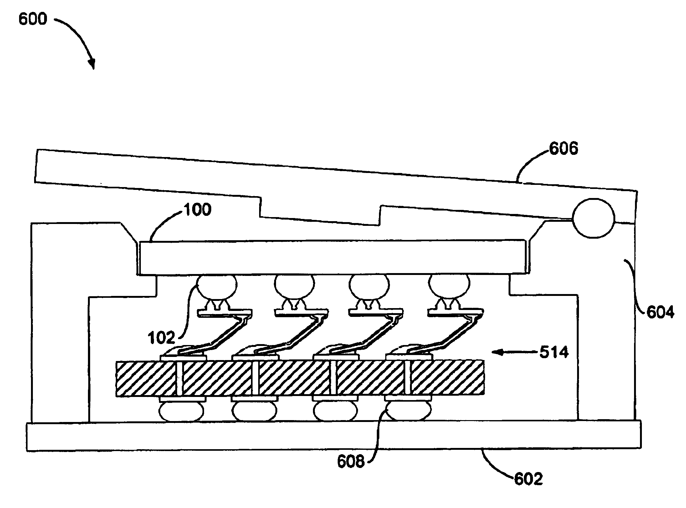
[0021]Embodiments of the invention provide an interconnect structure that is inexpensively manufactured and easily insertable into a socket. The interconnect structure is manufactured by forming a sacrificial substrate with cavities that is covered by a masking material having openings corresponding to the cavities. A first plating process is performed by depositing conductive material, followed by coupling wires within the openings and performing another plating process by depositing more conductive material. The interconnect structure is completed by first removing the masking material and sacrificial substrate. Ends of the wires are coupled opposite now-formed contact structures to a board. To complete the socket, a support device is coupled to the board to hold a tested integrated circuit.

Integrated Circuit Semiconductor

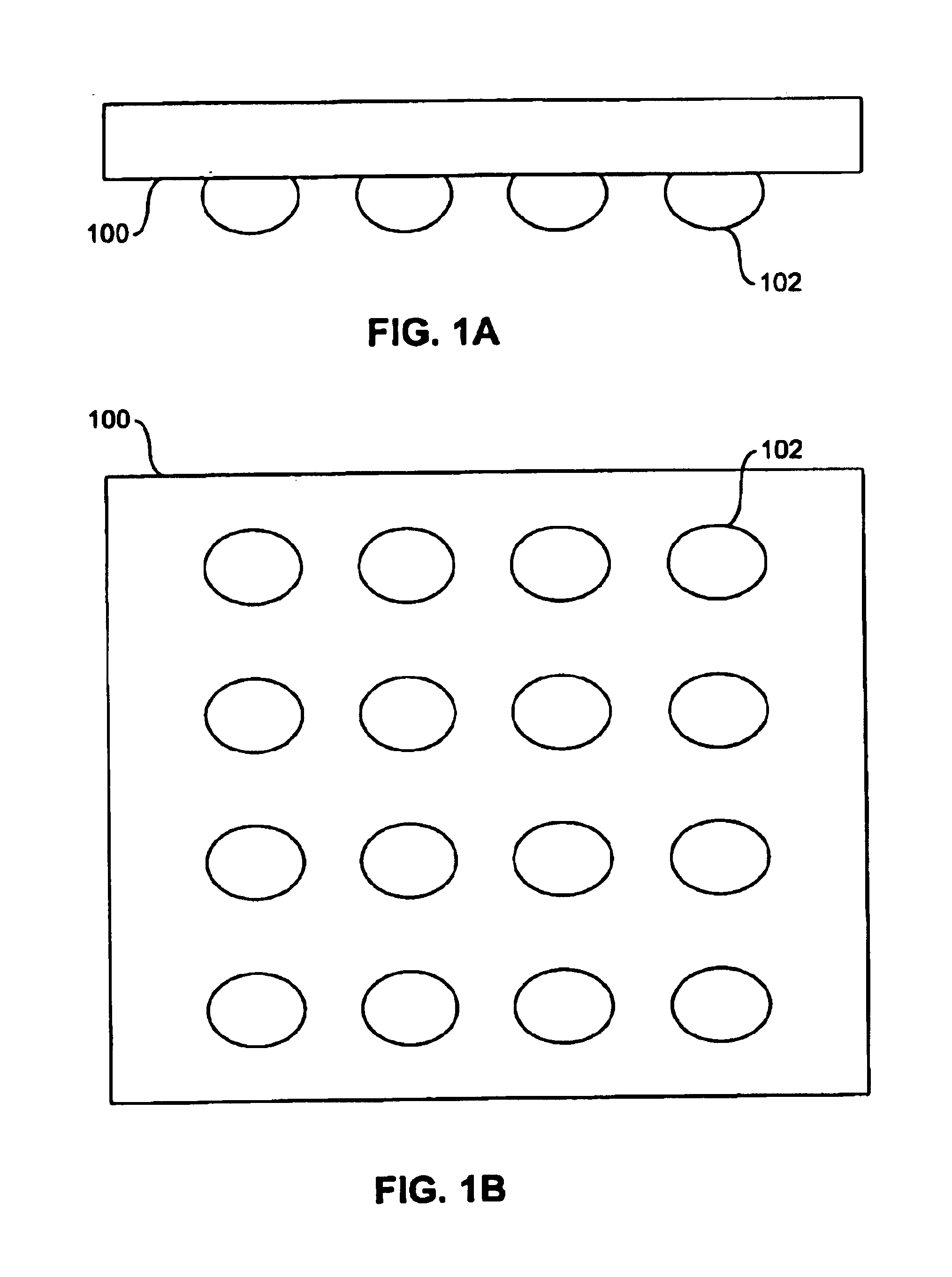
[0022]FIGS. 1A-1B show side and bottom views, respectively, of a semiconductor chip 100 (e.g., an integrated circuit (IC)) that is to be tested according to embo...


PUM

PropertyMeasurementUnit
diameteraaaaaaaaaa
thickaaaaaaaaaa
conductiveaaaaaaaaaa

Abstract

A interconnect structure is inexpensively manufactured and easily insertable into a socket. The interconnect structure is manufactured by forming a sacrificial substrate with cavities that is covered by a masking material having openings corresponding to the cavities. A first plating process is performed by depositing conductive material, followed by coupling wires within the openings and performing another plating process by depositing more conductive material. The interconnect structure is completed by first removing the masking material and sacrificial substrate. Ends of the wires are coupled opposite now-formed contact structures to a board. To complete the socket, a support device is coupled to the board to hold a tested integrated circuit.

Description

BACKGROUND OF THE INVENTION[0001]1. Field of the Invention[0002]This invention is directed to a socket for an integrated circuit. More particularly, the socket is a test or burn-in socket for connecting an integrated circuit to a tester for final testing or a burn-in board for burn-in.[0003]2. Background Art[0004]Testing of semiconductor chips is an important operation in semiconductor manufacturing. Different types of tests are performed at different stages of a semiconductor chip manufacturing process. For example, initial tests can be performed on a wafer scale when semiconductor chips have been fabricated on a wafer, but have not yet been diced and packaged. These initial tests may help to identify defective chips prior to performing more expensive and time consuming packaging steps. After the initial testing, a wafer is diced and individual semiconductor chips are packaged. More exacting tests and burn-in operations are then performed on a chip scale to evaluate individual semi...

Claims


Application Information

Patent Timeline
Patent Type & Authority Patents(United States)
IPC IPC(8): G01R1/04G01R1/02G01R3/00G01R1/073
CPCG01R1/0433G01R1/07378G01R3/00G01R31/2863G01R1/0483Y10T29/49197H01L2924/01046H01L2924/01078H01L2924/01079H01L2924/14H01L2924/01055H01L24/13H01L2224/131Y10T29/4921Y10T29/49224Y10T29/49149Y10T29/49169Y10T29/53265Y10T29/4913Y10T29/49144Y10T29/53217Y10T29/49179Y10T29/49211Y10T29/49117Y10T29/49204H01L2924/014H01L22/00
Inventor KHANDROS, IGOR Y.MATHIEU, GAETAN L.REYNOLDS, CARL V.
Owner FORMFACTOR INC
Why Eureka
Try Eureka