
Revolution member supporting apparatus and semiconductor substrate processing apparatus

a technology of supporting apparatus and semiconductor substrate, which is applied in the direction of sealing devices, manufacturing tools, lapping machines, etc., can solve the problems of slipping of the wafer at the engaging portion, inability to carry out satisfactory cleaning treatment, and inability to hold the wafer sufficiently strong

Inactive Publication Date: 2005-07-26
EBARA CORP
View PDF21 Cites 45 Cited by
  • Summary
  • Abstract
  • Description
  • Claims
  • Application Information

AI Technical Summary

Benefits of technology

"The present invention provides a revolution member supporting apparatus for a semiconductor substrate processing apparatus that can securely hold and rotate the substrate, allowing for cleaning and polishing of the substrate. The apparatus is compact, requires minimal space, and can be easily installed and maintained. Additionally, the invention provides a semiconductor substrate processing apparatus that can form circuit interconnects quickly and at low cost. The apparatus is also suitable for small-scale production and can flexibly adapt to changes in product demand."

Problems solved by technology

Accordingly, there has been the problem that a cleaning liquid cannot reach adequately into the engaging portions, and therefore a satisfactory cleaning treatment cannot be carried out.
This approach, however, has the problem that since the number of holding members in engagement with a semiconductor wafer is relatively small, the wafer cannot be held sufficiently firmly, whereby slipping of the wafer at the engaging portions is likely to occur.
This may wear the holding members and produce particles that contaminate the semiconductor wafer.
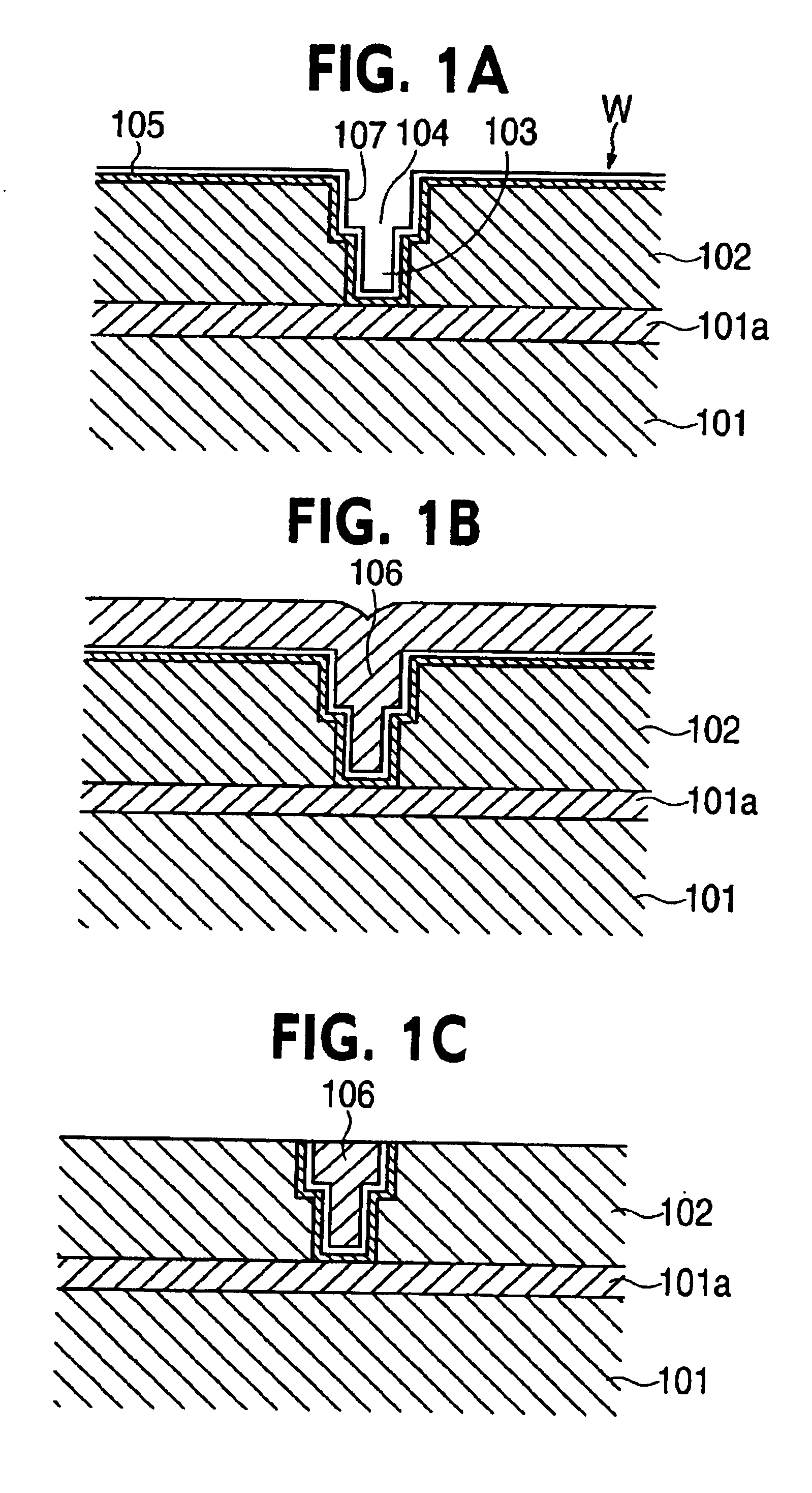
Copper can easily be diffused into the oxide film 102 in a semiconductor fabrication process such as annealing, for example, thus deteriorating the electric insulation of the oxide film and impairing the adhesiveness of the oxide film with a film to be subsequently deposited to possibly cause separation of the deposited film.
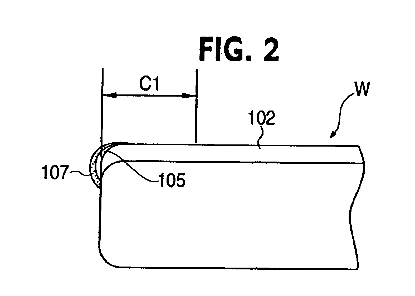
Furthermore, copper deposited on the outer peripheral portion of the substrate other than the circuit formation area is not only unnecessary, but may cause cross contamination in subsequent processes of delivering, storing and processing the semiconductor substrate.
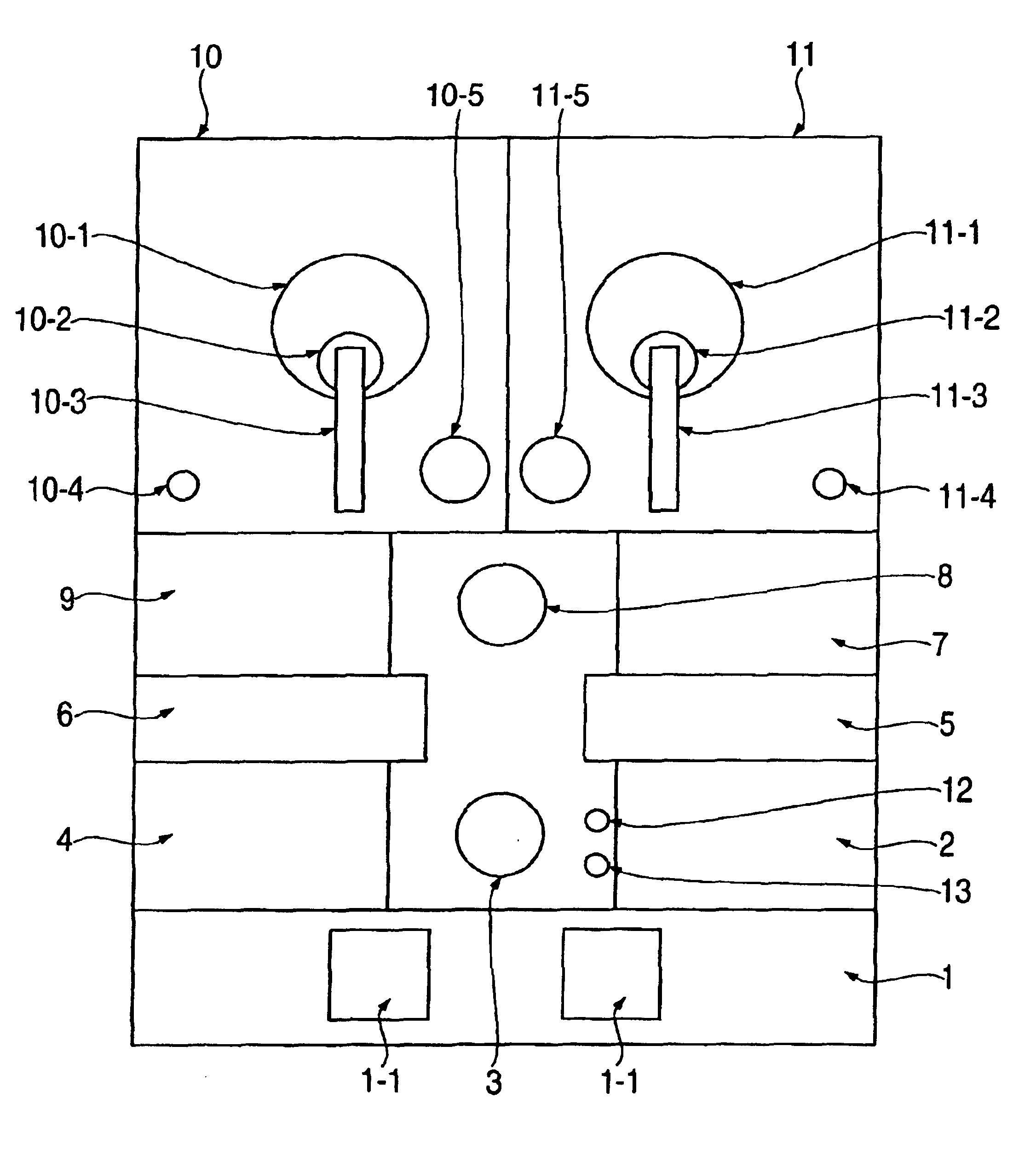
Thus, there have been problems that the initial cost and the running cost for the apparatuses are high, installation spaces for installation of both apparatuses need to be wide, and a long processing time is required.

Method used


Image

  • Revolution member supporting apparatus and semiconductor substrate processing apparatus
  • Revolution member supporting apparatus and semiconductor substrate processing apparatus
  • Revolution member supporting apparatus and semiconductor substrate processing apparatus

Examples


Embodiment Construction

[0122]Embodiments of the present invention will now be described with reference to the drawings. FIGS. 3 through 6 show an embodiment of a revolution member supporting apparatus in accordance with the present invention. The revolution member supporting apparatus 40 is for holding a substrate (object to be rotated) W such as a semiconductor wafer, and has a disc-shaped rotatable member 44 that is set horizontally and rotated by a rotatable drive shaft 42, and a plurality of holding members 46 for holding the substrate W above the rotatable member 44. The holding members 46 are mounted on the peripheral portion of the rotatable member 44 and arranged along a circle with the rotatable drive shaft 42 as a center, with each two adjacent members being spaced at a predetermined distance (60° in the embodiment of FIG. 4). The holding members 46 engage the periphery W′ of the substrate W, thereby holding the substrate W horizontally. In FIG. 3, reference numeral 47 denotes a belt driving dev...


PUM

PropertyMeasurementUnit
optical film thickness measuringaaaaaaaaaa
diameteraaaaaaaaaa
distanceaaaaaaaaaa

Abstract

A revolution member supporting apparatus holds and rotates a disc-shaped object (object to be rotated) such as a semiconductor wafer. The revolution member supporting apparatus includes a rotatable member which rotates about an axis of roation, and a plurality of holding members which are disposed along a circle having a center corresponding to the axis of rotation of the rotatable member, and which revolve around the axis of rotation when the rotatable member rotates, wherein the holding members are allowed to swing about their own central axes.

Description

BACKGROUND OF THE INVENTION[0001]1. Field of the Invention[0002]The present invention relates to a revolution member supporting apparatus for holding and rotating a disc-shaped object (object to be rotated) such as a semiconductor wafer. The present invention also relates to a semiconductor substrate processing apparatus for forming circuit interconnects by filling a circuit pattern trench and / or hole formed in a semiconductor substrate with a plated metal film, and removing the plated metal film while leaving the metal film at the filled portion.[0003]2. Description of the Related Art[0004]For example, a semiconductor wafer, which has undergone a copper-plating treatment or a CMP (chemical mechanical polishing) treatment, is generally subjected to a cleaning treatment. The cleaning treatment is usually performed by supplying a cleaning liquid onto the upper surface of a semiconductor wafer around its center, while the wafer is being held horizontally and rotated by a revolution mem...

Claims


Application Information

Patent Timeline
Patent Type & Authority Patents(United States)
IPC IPC(8): B24B37/04H01L21/687H01L21/00H01L21/67B24B37/34
CPCB24B37/345C25D17/06H01L21/67046H01L21/67051H01L21/6715H01L21/67167H01L21/67173H01L21/67184H01L21/6719H01L21/67201H01L21/67253H01L21/67742H01L21/67748H01L21/67766H01L21/68707H01L21/68728C25D17/004C25D7/123C25D17/001H01L21/68
Inventor HONGO, AKIHISAKATAKABE, ICHIROMORISAWA, SHINYA
Owner EBARA CORP
Learn More