Die surface magnetic field shield

a magnetic field shield and surface technology, applied in the direction of semiconductor/solid-state device details, digital storage, instruments, etc., can solve the problems of adversely affecting the functionality of the device, and affecting the operation of the device, so as to reduce the manufacturing cost and improve the production yield , the effect of low magnetic field

Inactive Publication Date: 2005-07-26
INTELLECTUAL VENTURES ASSETS 186 LLC
View PDF6 Cites 16 Cited by
  • Summary
  • Abstract
  • Description
  • Claims
  • Application Information

AI Technical Summary

Benefits of technology

[0014]There may be several advantages for forming a topography with a MFS layer as described herein. For example, a topography with such a layer may be protected from external magnetic field vectors present within the ambient of the topography. In addition, such an MFS layer may advantageously retain the magnetic field vectors generated by the circuitry of a topography. Such retention of magnetic field vectors may allow a lower magnetic field to be applied to the memory cell, since the strength of the generated magnetic field will not dissipate. In some embodiments, an MFS layer as described herein may be used for shielding portions of a topography. In such an embodiment, the topography may advantageously have a relativel

Problems solved by technology

In particular, the ambient to which a device is exposed may affect the operation of a device.
For example, exposure to extremely low or high temperatures may adversely affect the operation of a device.
In addition or alternatively, the presence of stray or external magnetic fields may affect the functionality of a device.
In particular, exposure to external magnetic fields may be particularly harmful for devices that include magnetoresistive memory cells, such as giant magnetoresistance (GMR) memory cells or magnetic tunnel junction (MTJ) memory cells.
External or stray magnetic

Method used


Image

  • Die surface magnetic field shield
  • Die surface magnetic field shield
  • Die surface magnetic field shield

Examples


Embodiment Construction

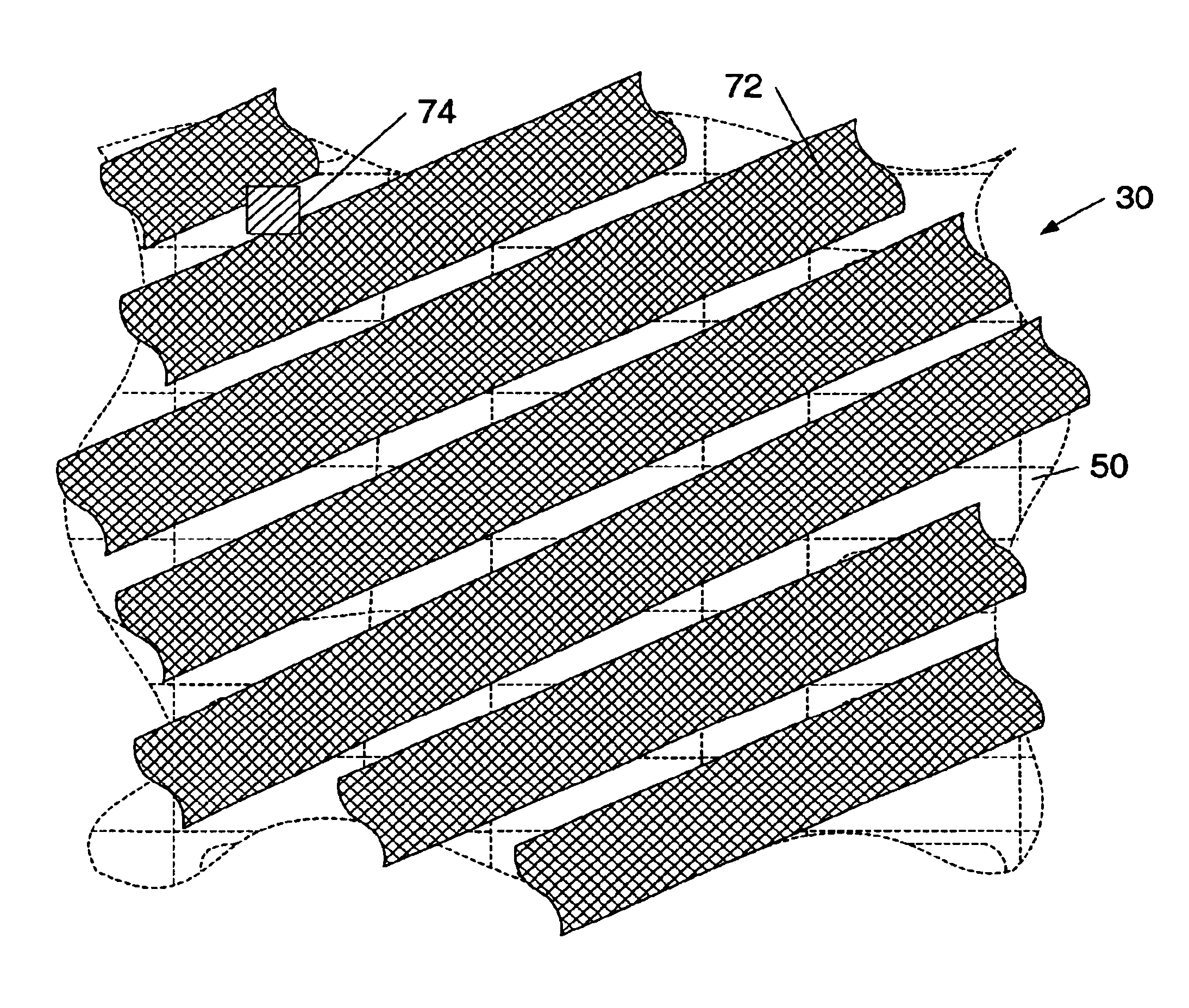
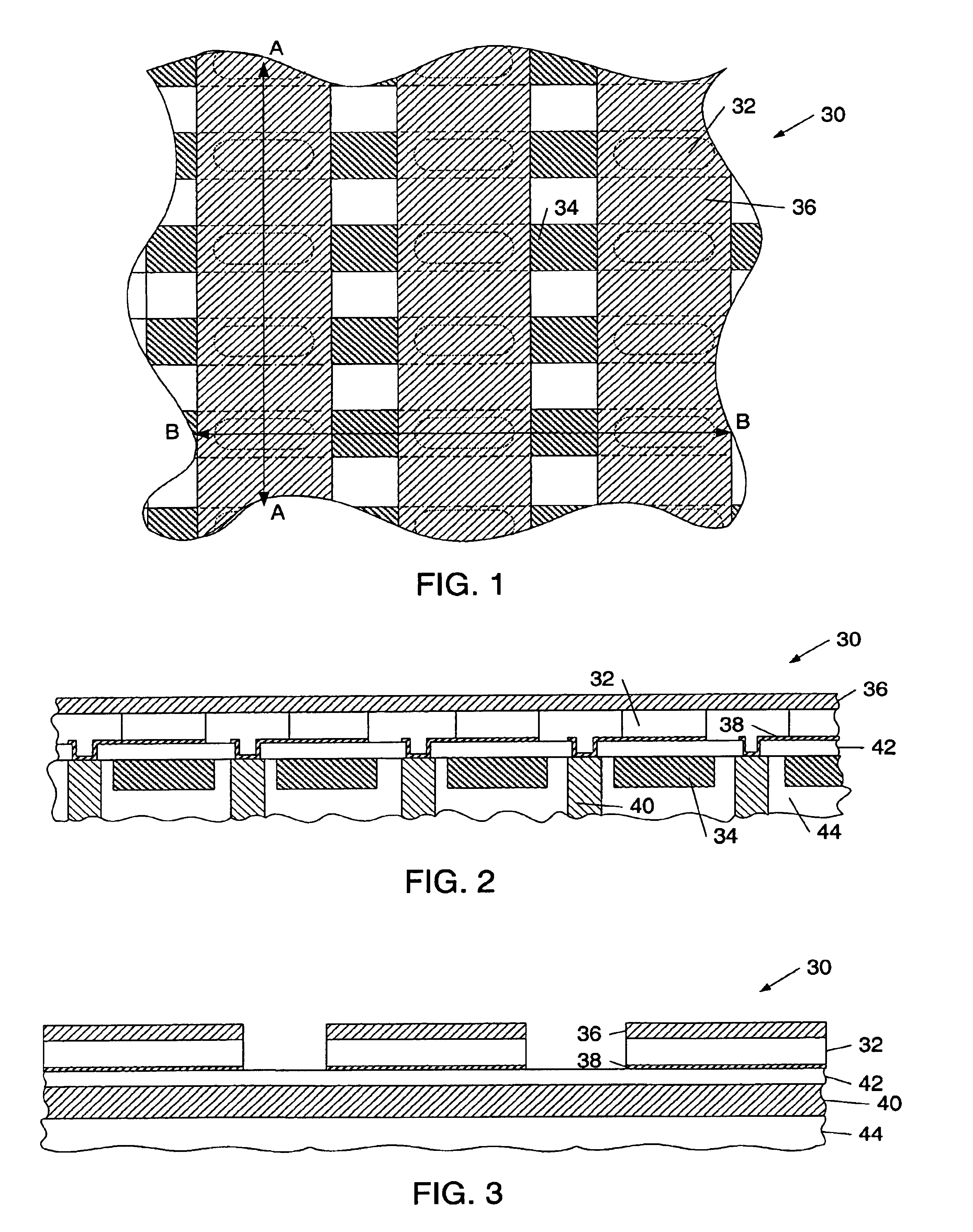
[0044]Turning to the drawings, exemplary embodiments of methods for processing a semiconductor topography are shown in FIGS. 1-26. In particular, methods for forming a magnetic field shield (MFS) layer upon a semiconductor topography are provided. FIG. 1 depicts a partial top view of semiconductor topography 30 in which a plurality of memory cells 32 have been arranged between a plurality of digit lines 34 and a plurality of bit lines 36. A partial cross-sectional view of semiconductor topography 30 along line AA is shown in FIG. 2. In contrast, a partial cross-sectional view of semiconductor 30 along line BB is shown in FIG. 3. As shown in FIGS. 1-3, bit lines 36 overly memory cells 32 and respective underlying portions of digit lines 34. As such, memory cells 32 and respective underlying portions of digit lines 34 are represented by dashed lines in FIG. 1, indicating that they are arranged below bit lines 36. In addition, bit lines 36 are arranged perpendicular to the direction to...


PUM


Abstract

A semiconductor topography is provided which includes a magnetic field shield layer formed upon a semiconductor device. In particular, the semiconductor topography may include a ferromagnetic layer adapted to shield underlying layers from external magnetic fields. Such a ferromagnetic layer may include either ferrite and/or non-ferrite materials. In some embodiments, the semiconductor topography may include a magnetic field shield layer with a different pattern configuration than an adjacent passivation layer. Consequently, a method for processing a semiconductor topography which includes patterning a magnetic field shield layer to form openings other than bond pad openings within the semiconductor topography is provided.

Description

BACKGROUND OF THE INVENTION[0001]1. Field of the Invention[0002]This invention relates to semiconductor device manufacturing, and more particularly, to a magnetic field shield layer and a method for making the same.[0003]2. Description of the Related Art[0004]The following descriptions and examples are given as background only.[0005]Several conditions may affect the operation of a semiconductor device. In particular, the ambient to which a device is exposed may affect the operation of a device. For example, exposure to extremely low or high temperatures may adversely affect the operation of a device. In addition or alternatively, the presence of stray or external magnetic fields may affect the functionality of a device. In particular, exposure to external magnetic fields may be particularly harmful for devices that include magnetoresistive memory cells, such as giant magnetoresistance (GMR) memory cells or magnetic tunnel junction (MTJ) memory cells. In general, magnetoresistive mem...

Claims


Application Information

Patent Timeline
IPC IPC(8): H01L23/552G11C11/16H01L27/22H01L43/02
CPCG11C11/16H01L23/552H01L27/222H01L2924/0002H01L2924/00H10B61/00
Inventor RAY, OINDRILAJENNE, FREDERICK B.
Owner INTELLECTUAL VENTURES ASSETS 186 LLC
Why Eureka
Try Eureka