FET channel having a strained lattice structure along multiple surfaces

a lattice structure and fet technology, applied in the field of layered structure, can solve the problems of limiting the further scaling of fets, requiring greater control, and current leakage continuing to be a limiting factor

Inactive Publication Date: 2005-07-26
MICROSOFT TECH LICENSING LLC
View PDF9 Cites 326 Cited by
  • Summary
  • Abstract
  • Description
  • Claims
  • Application Information

AI Technical Summary

Benefits of technology

[0011]The channel envelope is in contact with the opposed sidewall surfaces and the top surface of the channel core. The channel envelope is formed from a second semiconductor material defining a second lattice structure that differs from the first lattice structure. This difference in lattice structure provides enhanced electrical conductivity due to stretching or compressing of the lattice structure. Preferably, the two materials are silicon and a silicon-germanium compound.

Problems solved by technology

Semiconductors and integrated circuit chips have become ubiquitous within many products due to their continually decreasing cost and size.
However, such small scaling necessitates greater control over performance issues such as short channel effects, punch-through, and MOS leakage current.
However, current leakage continues to be a limiting factor in further scaling of FETs toward the atomic limit.

Method used


Image

  • FET channel having a strained lattice structure along multiple surfaces
  • FET channel having a strained lattice structure along multiple surfaces
  • FET channel having a strained lattice structure along multiple surfaces

Examples


Embodiment Construction

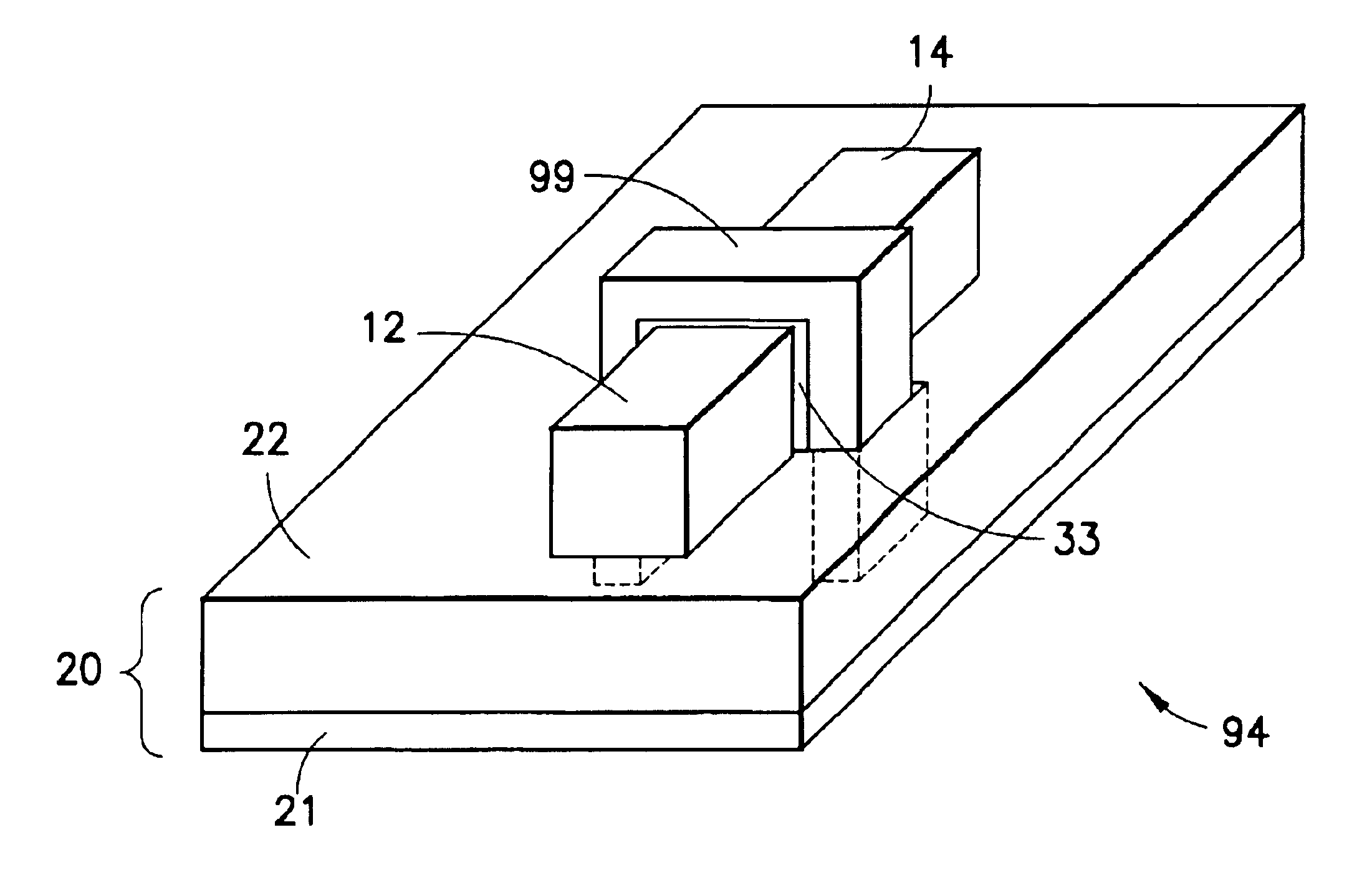
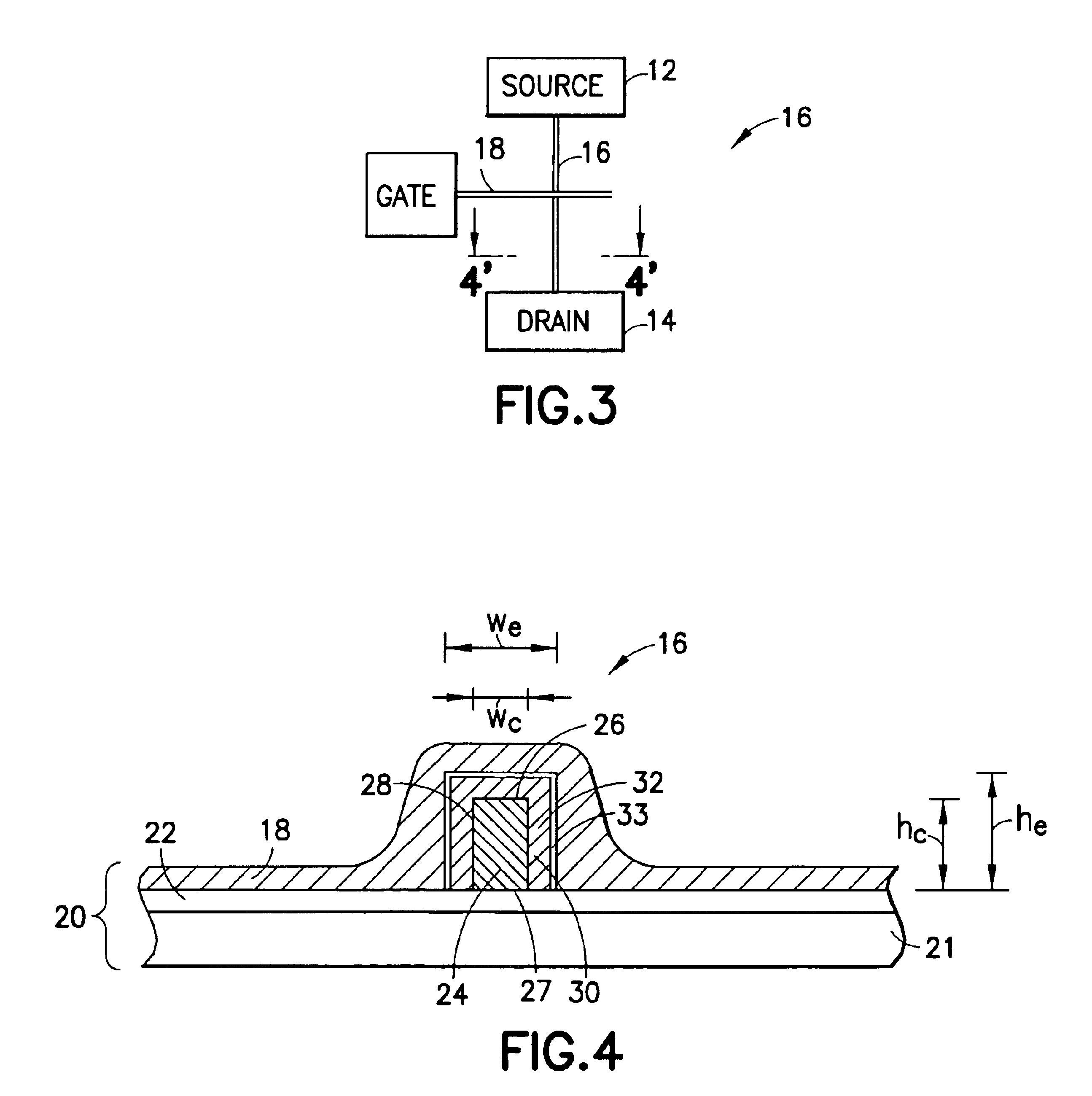
[0010]The foregoing and other problems are overcome, and other advantages are realized, in accordance with the presently preferred embodiments of these teachings. The present invention concerns a channel for electrically connecting a source and a drain of a field effect transistor (FET), commonly called a fin for a FinFET. The channel includes a channel core and a channel envelope. The channel core is coupled to a substrate such as a SIMOX wafer (a wafer with an upper region separated by implanted oxygen) or bonded wafer. The channel core defines a top surface that is spaced from the substrate, and opposed sidewall surfaces between the substrate and the top surface. The channel core is formed from a first semiconductor material defining a first lattice structure.

[0011]The channel envelope is in contact with the opposed sidewall surfaces and the top surface of the channel core. The channel envelope is formed from a second semiconductor material defining a second lattice structure tha...


PUM


Abstract

A channel 16 of a FinFET 10 has a channel core 24 and a channel envelope 32, each made from a semiconductor material defining a different lattice structure to exploit strained silicon properties. A gate is coupled to the channel envelope through a gate dielectric. Exemplary materials are Si and SixGe1-x, wherein 78<x<92. The channel core 24 has a top surface 26 of width wc and an upstanding surface 28, 30 of height hc, preferably oriented 90° to one another. The channel envelope 32 is in contact with the top 26 and upstanding surfaces 28, 30 so that the area of interface is increased as compared to contact only along the top surface 26, improving electrical conductivity and gate 18 control over the channel 16. The height hc can be tailored to enable a smaller scale FET 10 within a stabilized SRAM. Various methods of making the channel 16 are disclosed, including a mask and etch method, a handle wafer / carrier wafer method, and a shallow trench method. Embodiments and methods for FinFETs with one to four gates are disclosed.

Description

TECHNICAL FIELD[0001]These teachings relate generally to field effect transistors (FET) disposed on a semiconductor wafer or chip, in particular, to a layered structure as a channel that connects a source and a drain of a FET, wherein one of the layers is characterized by a strained lattice structure.BACKGROUND OF THE INVENTION[0002]Semiconductors and integrated circuit chips have become ubiquitous within many products due to their continually decreasing cost and size. Miniaturization in general allows increased performance (more processing per clock cycle and less heat generated) at lower power levels and lower cost. Present technology is at or approaching atomic-level scaling of certain micro-devices such as logic gates, FETs, capacitors, etc. Circuit chips with hundreds of millions of such devices are not uncommon. Further size reductions appear to be approaching the physical limit of trace lines and micro-devices that are embedded upon and within their semiconductor substrates. ...

Claims


Application Information

Patent Timeline
Patent Type & Authority Patents(United States)
IPC IPC(8): H01L29/06H01L27/11H01L29/02H01L31/102H01L31/072H01L31/0264H01L31/0328H01L31/0336H01L27/01H01L31/06H01L31/109H01LH01L21/336H01L21/8244H01L21/84H01L27/12H01L29/786
CPCH01L21/84H01L21/845H01L27/11H01L27/1108H01L27/1203H01L27/1211H01L29/42392H01L29/66795H01L29/785H01L29/78687H01L27/1207Y10S257/903H10B10/00H10B10/125H01L29/04H01L29/7842
Inventor JOSHI, RAJIV VWILLIAMS, RICHARD Q
Owner MICROSOFT TECH LICENSING LLC
Why Eureka
Try Eureka