Organic light emitting diode and method for producing the same

a light-emitting diode and organic technology, applied in the field of polymer oled, can solve the problem that the photo-resist structure only provides lateral border limitations for the channel, and achieves the effect of reducing the number of lateral borders

Inactive Publication Date: 2005-08-02
SAMSUNG DISPLAY CO LTD
View PDF15 Cites 19 Cited by
  • Summary
  • Abstract
  • Description
  • Claims
  • Application Information

AI Technical Summary

Benefits of technology

[0022]To solve the above-described problems, it is an object of the present invention to provide an organic light emitting diode (OLED) which can prevent ink from a hole transport layer (HTL) or polymer layer from running out from channels and in which the HTL or polymer layer has a uniform layer thickness.

Problems solved by technology

The photo-resist structures only provide lateral border limitations for the channels.

Method used


Image

  • Organic light emitting diode and method for producing the same
  • Organic light emitting diode and method for producing the same
  • Organic light emitting diode and method for producing the same

Examples


Embodiment Construction

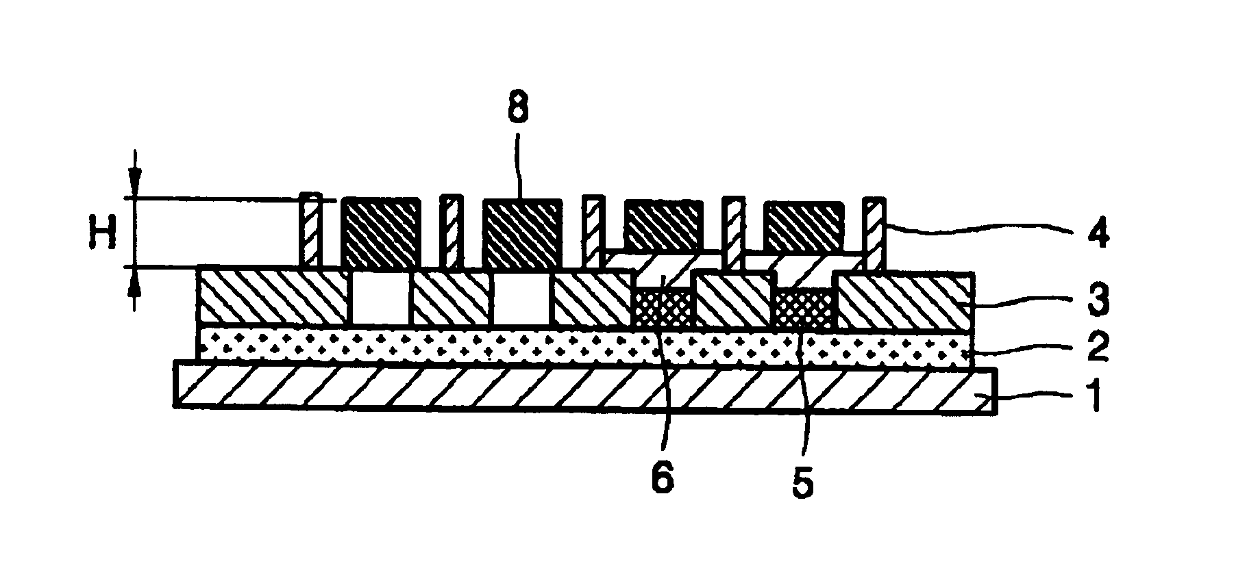
[0038]Preferred embodiments of the present invention will now be described in detail with reference to the accompanying drawings. An explanation will be given with the example of a passive matrix type polymer OLED. Although not shown in the drawings, the invention can also be applied to active matrix type polymer OLED.

[0039]FIGS. 3A and 3B show the state in which HTL ink and polymer ink are printed onto a substrate according to one embodiment of the invention.

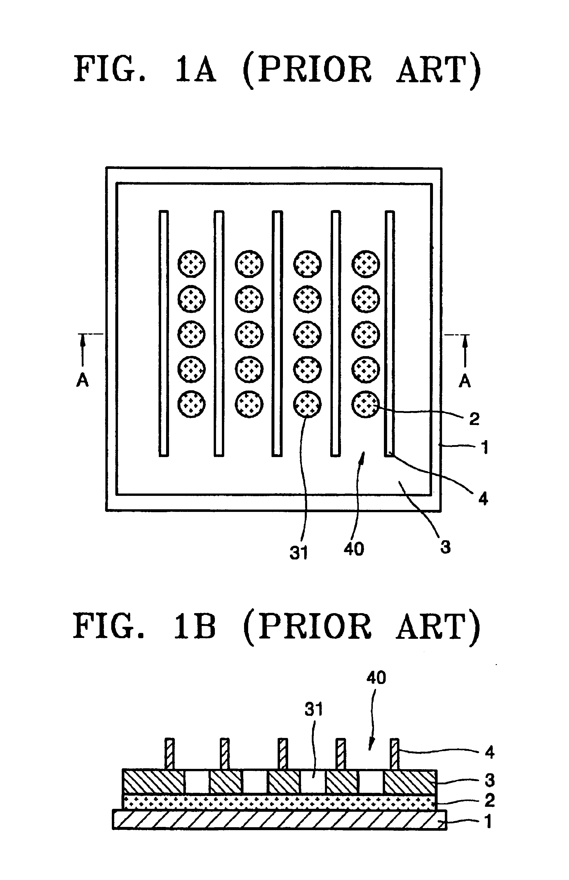
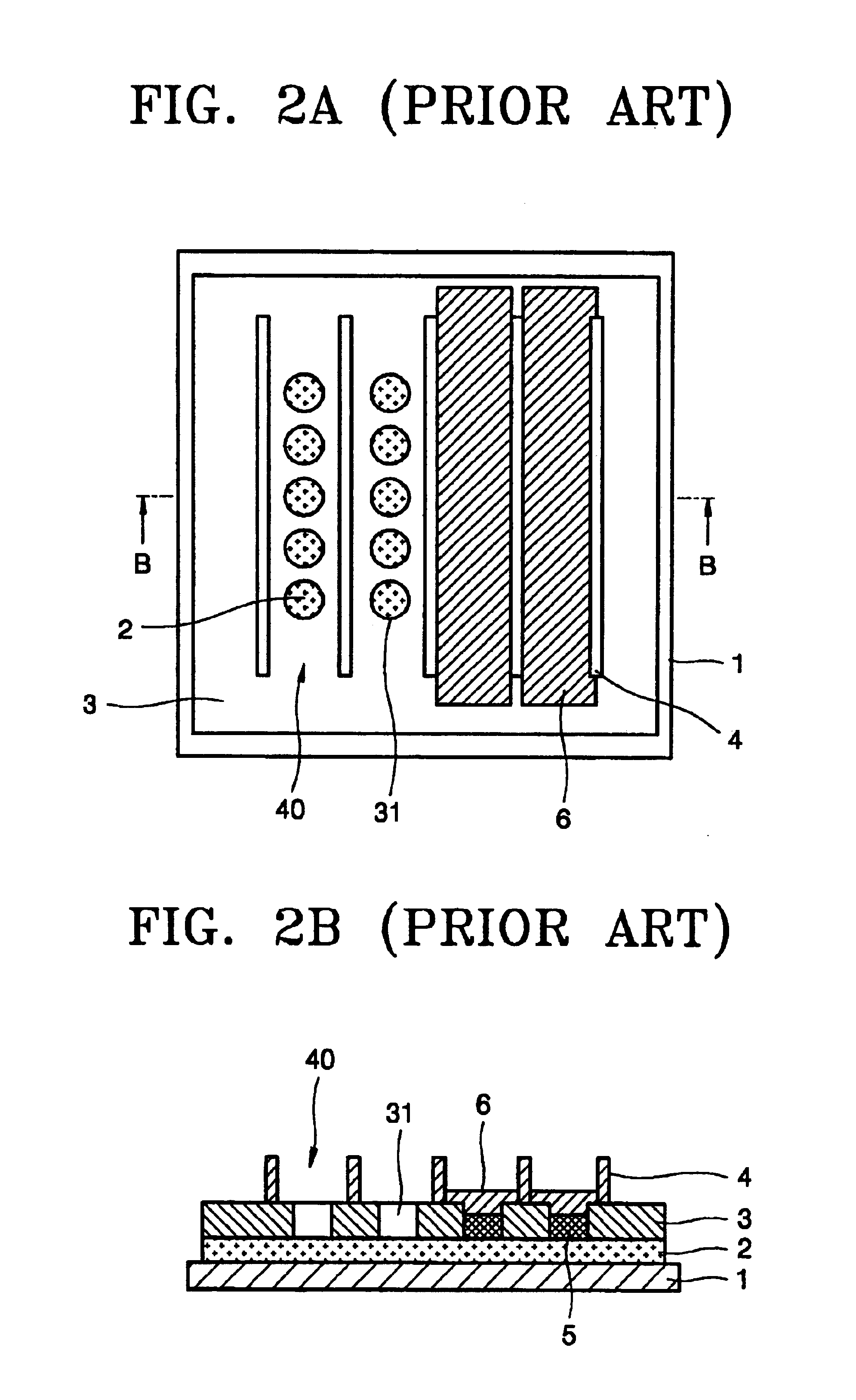
[0040]The structure of the substrate shown in FIGS. 3A and 3B is substantially the same as that of the conventional substrate shown in FIGS. 1A and 1B. The same elements are denoted by the same reference numerals.

[0041]Referring to FIGS. 3A and 3B, a first electrode layer 2 is formed above a substrate 1 formed of a general glass plate. The first electrode layer 2 may be formed of a transparent conductor material, e.g., ITO. Although not shown, the first electrode layer 2 may be patterned in a predetermined pattern. The distance...


PUM


Abstract

An organic light emitting diode (OLED) includes a substrate having a first electrode layer formed thereon in a predetermined pattern, an insulator layer defining the upper portion of the substrate having the first electrode layer in a predetermined pattern, an organic polymer layer formed based on the pattern defined by the insulator layer, a barrier for blocking flow of the organic polymer layer at both ends of the pattern defined by the insulator layer, and a second electrode layer formed on the organic polymer layer.

Description

CROSS REFERENCE[0001]This application is a continuation application of Applicant's U.S. patent application Ser. No. 10 / 317,166 filed on Dec. 12, 2002, now U.S. Pat. No. 6,774,392, which is herein specifically incorporated by reference in its entirety.BACKGROUND OF THE INVENTION[0002]1. Field of the Invention[0003]The present invention relates to an organic light emitting diode (OLED) for realizing a full-color display device, and more particularly, to a polymer OLED and a method for producing the same.[0004]2. Description of the Related Art[0005]OLEDs which can realize full-color display devices are largely divided into two types: OLEDs employing low molecular weight materials; and OLEDs employing polymer high molecular weight materials.[0006]A high molecular weight OLED is generally fabricated such that two opposite electrodes, a cathode and an anode, are disposed on a substrate. A hole transport layer (HTL) and an emission layer are provided between the anode and the cathode. In t...

Claims


Application Information

Patent Timeline
Patent Type & Authority Patents(United States)
IPC IPC(8): H01L27/32H01L27/28H05B33/22H01L51/40
CPCH01L27/3283H01L27/3246H01L51/0004H10K59/122H10K59/173H10K71/13H05B33/22
Inventor HUMBS, WERNERUHLIG, ALBRECHTSCHADIG, MARCUS
Owner SAMSUNG DISPLAY CO LTD
Why Eureka
Try Eureka