Semiconductor package exhibiting efficient lead placement

a technology of semiconductors and lead placement, applied in the direction of semiconductor devices, semiconductor/solid-state device details, electrical apparatus, etc., can solve the problems of limited surface area available to accommodate and significantly affect the number of leads provided, and achieve the effect of efficient lead placement in such a packag

Inactive Publication Date: 2005-08-09
AMKOR TECH SINGAPORE HLDG PTE LTD
View PDF213 Cites 132 Cited by
  • Summary
  • Abstract
  • Description
  • Claims
  • Application Information

AI Technical Summary

Benefits of technology

[0010]In one embodiment, an integrated circuit chip package is provided having an integrated circuit die bonded to portions of the top surfaces of leads. As a result of bonding the die to the leads rather than to only a separate die paddle, the leads are caused to partially reside under the die. As a result, surface area that would otherwise be consumed by the leads can be used for other leads, thus making the placement of leads in such a package more efficient. The die can be further bonded to a separate die paddle if so desired.

Problems solved by technology

One of the drawbacks associated with certain MLF semiconductor packages is the limited surface area available to accommodate leads.
Unfortunately, conventional MLF designs typically require these leads to be located on the bottom surface of the semiconductor package around the perimeter of a die paddle portion of the lead frame.
Thus, the limited surface area available for lead placement on such packages can significantly impact the number of leads provided.

Method used


Image

  • Semiconductor package exhibiting efficient lead placement
  • Semiconductor package exhibiting efficient lead placement
  • Semiconductor package exhibiting efficient lead placement

Examples


Embodiment Construction

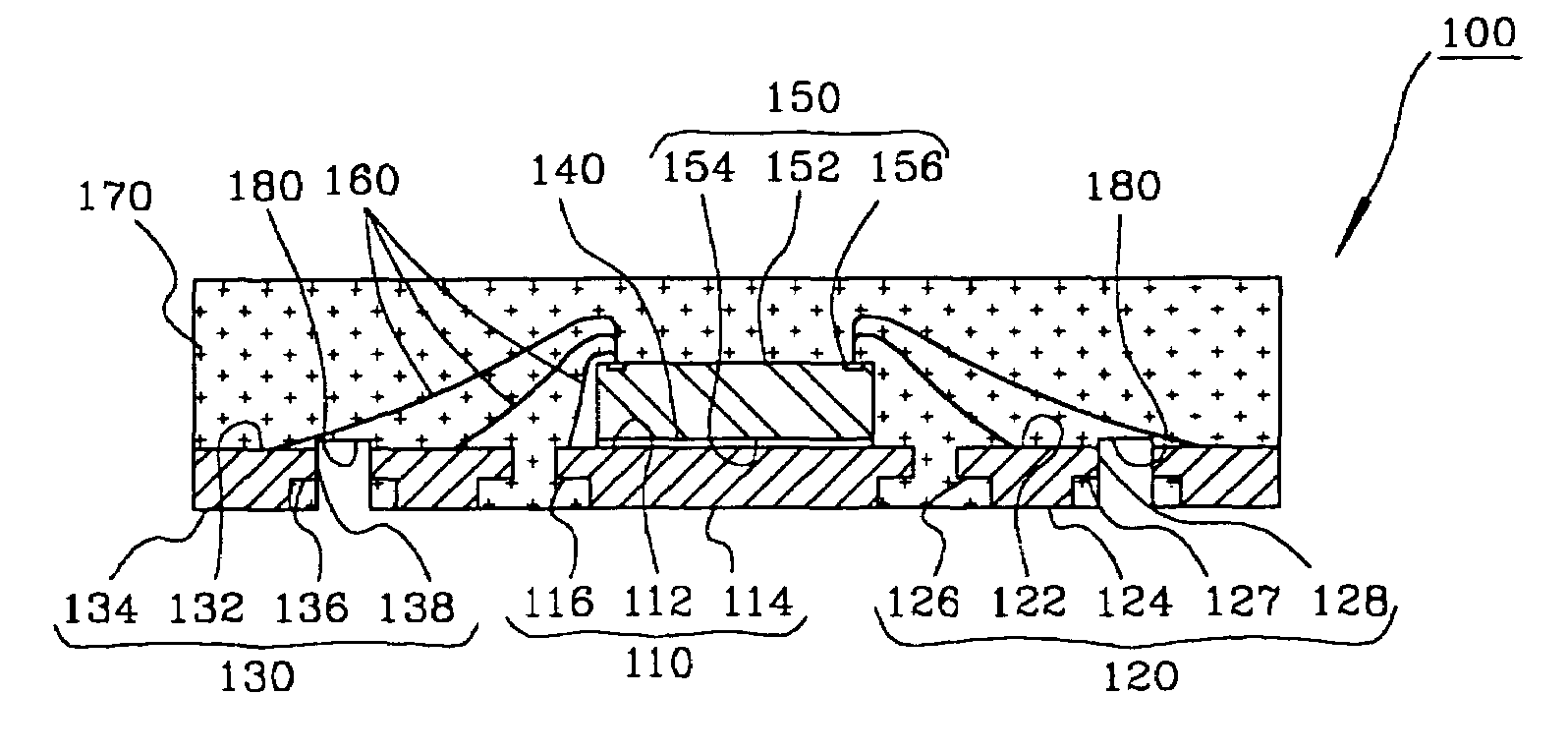
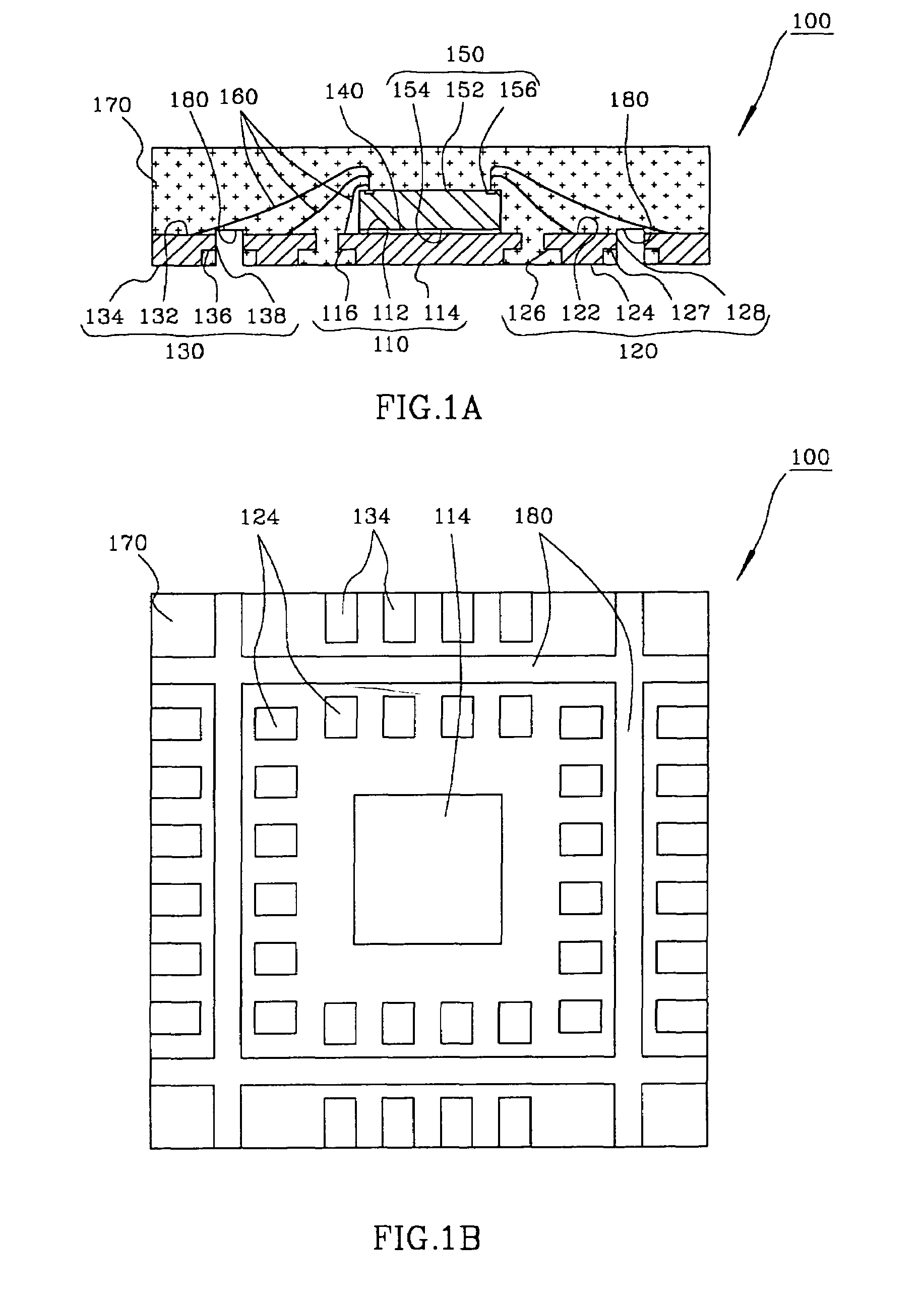
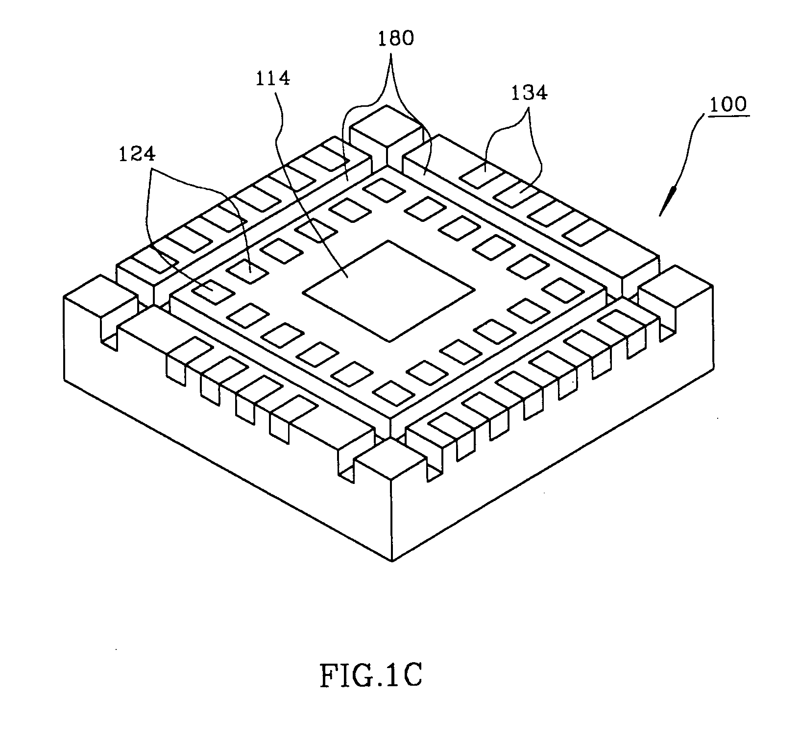
[0037]FIGS. 1A–C provide sectional, bottom, and perspective views of a semiconductor package having multiple leads separated by channels. As shown in the drawings, semiconductor package 100 includes a substantially planar die paddle 110, a plurality of first leads 120, a plurality of second leads 130, an integrated circuit die 150 bonded to the die paddle 110, and conductive wires 160 for electrically connecting the integrated circuit die 150 to the first and second leads 120 and 130. Encapsulant 170 is provided for encapsulating die paddle 110, leads 120 and 130, integrated circuit die 150, and conductive wires 160. In addition, portions of leads 120 and 130 are exposed in an exterior surface of the encapsulant 170.

[0038]Die paddle 110 includes substantially planar top and bottom surfaces 112 and 114. Portions of bottom surface 114 are etched to form substantially planar partially etched surfaces 116. As a result, the area of bottom surface 114 is reduced in relation to the area of...


PUM


Abstract

A semiconductor package exhibiting efficient placement of semiconductor leads in a micro lead frame design is provided. An integrated circuit die is bonded to the top surfaces of leads, thereby allowing the leads to partially reside under the die. As a result, surface area on the bottom surface of the semiconductor package is recaptured. The die can be further bonded a die paddle if so desired. One or more channels can be cut into the bottom surface of the package in order to separate first and second leads. Such channels allow separate leads to be fabricated from a single lead member which is subsequently cut.

Description

CROSS-REFERENCE TO RELATED APPLICATIONS[0001](Not Applicable)STATEMENT RE: FEDERALLY SPONSORED RESEARCH / DEVELOPMENT[0002](Not Applicable)BACKGROUND OF THE INVENTION[0003]The present invention relates generally to integrated circuit chip package technology, and more particularly to a unique package design that facilitates the efficient placement of the leads therein.[0004]Integrated circuit dies are conventionally enclosed in plastic packages that provide protection from hostile environments and enable electrical interconnection between the integrated circuit die and an underlying substrate such as a printed circuit board (“PCB”).[0005]Semiconductor packages employing micro lead frames (“MLF”) typically include a metal lead frame (often made from copper (Cu)), an integrated circuit die, bonding material to attach the integrated circuit die to the lead frame, bond wires which electrically connect pads on the integrated circuit die to individual leads of the lead frame, and a hard plas...

Claims


Application Information

Patent Timeline
Patent Type & Authority Patents(United States)
IPC IPC(8): H01L23/52H01L23/02H01L23/495H01L23/04H01L23/48H01L29/40H01L23/31
CPCH01L23/3107H01L23/4951H01L23/49541H01L23/49548H01L24/32H01L24/49H01L24/97H01L24/45H01L2224/16245H01L2224/29007H01L2224/32014H01L2224/32145H01L2224/32245H01L2224/45124H01L2224/45139H01L2224/45144H01L2224/45147H01L2224/48091H01L2224/48247H01L2224/48257H01L2224/48471H01L2224/4945H01L2224/73265H01L2224/85191H01L2224/92H01L2224/92247H01L2224/97H01L2924/01005H01L2924/01006H01L2924/01013H01L2924/01029H01L2924/01047H01L2924/01075H01L2924/01079H01L2924/01082H01L2924/14H01L2924/18165H01L2924/00014H01L2224/85H01L2224/83H01L2924/00012H01L24/48H01L2924/01033H01L2924/014H01L2924/1815H01L2924/00H01L2224/48227H01L2924/181H01L24/73H01L2924/18301H01L2224/45015H01L2924/207
Inventor LEE, SUN GOOLEE, CHOON HEUNGLEE, SANG HO
Owner AMKOR TECH SINGAPORE HLDG PTE LTD
Why Eureka
Try Eureka