
Semiconductor device, display device, and method of manufacturing the same

a technology of semiconductor devices and display devices, applied in the direction of identification means, instruments, optics, etc., can solve the problems of non-uniform electric field and alignment defect of liquid crystal molecules, and achieve the effects of enhancing productivity, yield and reliability, and avoiding disconnection of pixel electrodes

Inactive Publication Date: 2005-08-16
SEMICON ENERGY LAB CO LTD
View PDF12 Cites 4 Cited by
  • Summary
  • Abstract
  • Description
  • Claims
  • Application Information

AI Technical Summary

Benefits of technology

[0014]Therefore, with the foregoing in mind, it is an object of the present invention to provide a configuration for eliminating disconnection of pixel electrodes caused by a change in shape of an interlayer insulating film at the ends of metal wiring and a method of manufacturing the same; and to enhance productivity, yield and reliability.
[0015]It is another object of the present invention to provide a configuration for preventing an alignment defect of liquid crystal molecules and a non-uniform electric field caused by the roughness of the upper surface of an interlayer insulating film, and to enhance productivity, yield and reliability.
[0016]It is still another object of the present invention to provide a configuration for preventing a defect of a light-emitting device in which a minute defect occurs in a light-emitting layer due to the roughness of a pixel electrode caused by the roughness of the upper surface of an interlayer insulating film and a method of manufacturing the same, and to enhance productivity, yield, and reliability.

Problems solved by technology

Disconnection of the pixel electrode at the ends of the wiring (Ti / Al / Ti) is one of the causes for a point defect of a semiconductor device.
There is also another problem.
Due to the roughness of the upper surface of the interlayer insulating film, the pixel electrode on the interlayer insulating film is roughened to cause an alignment defect of liquid crystal molecules and a non-uniform electric field.
Furthermore, due to the roughness of the upper surface of the interlayer insulating film, the pixel electrode on the interlayer insulating film is roughened to cause a defect of the light-emitting device in which a minute defect occurs in the light-emitting layer laminated on the pixel electrode.

Method used


Image

  • Semiconductor device, display device, and method of manufacturing the same
  • Semiconductor device, display device, and method of manufacturing the same
  • Semiconductor device, display device, and method of manufacturing the same

Examples


embodiment mode 1

[Embodiment Mode 1]

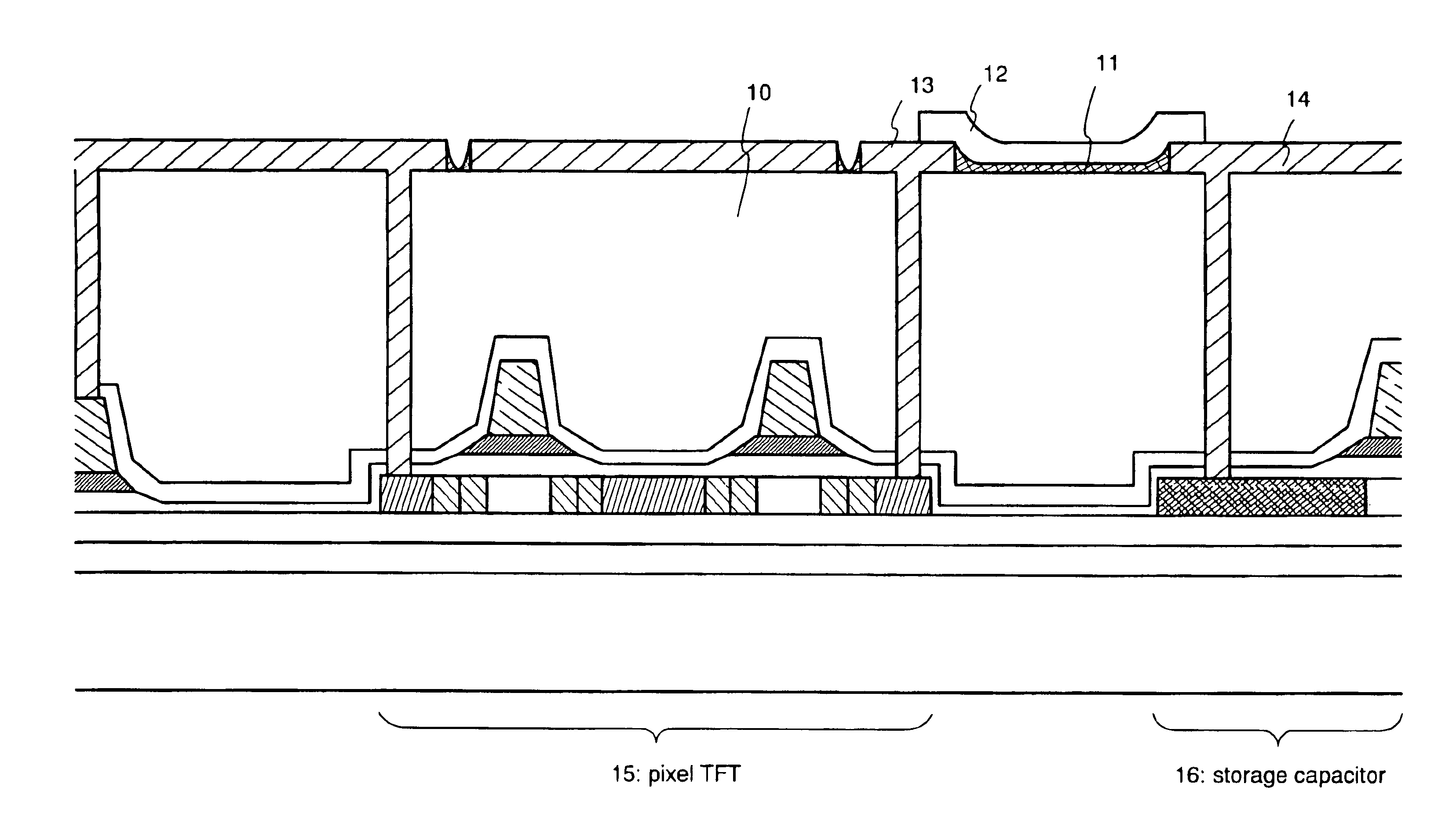
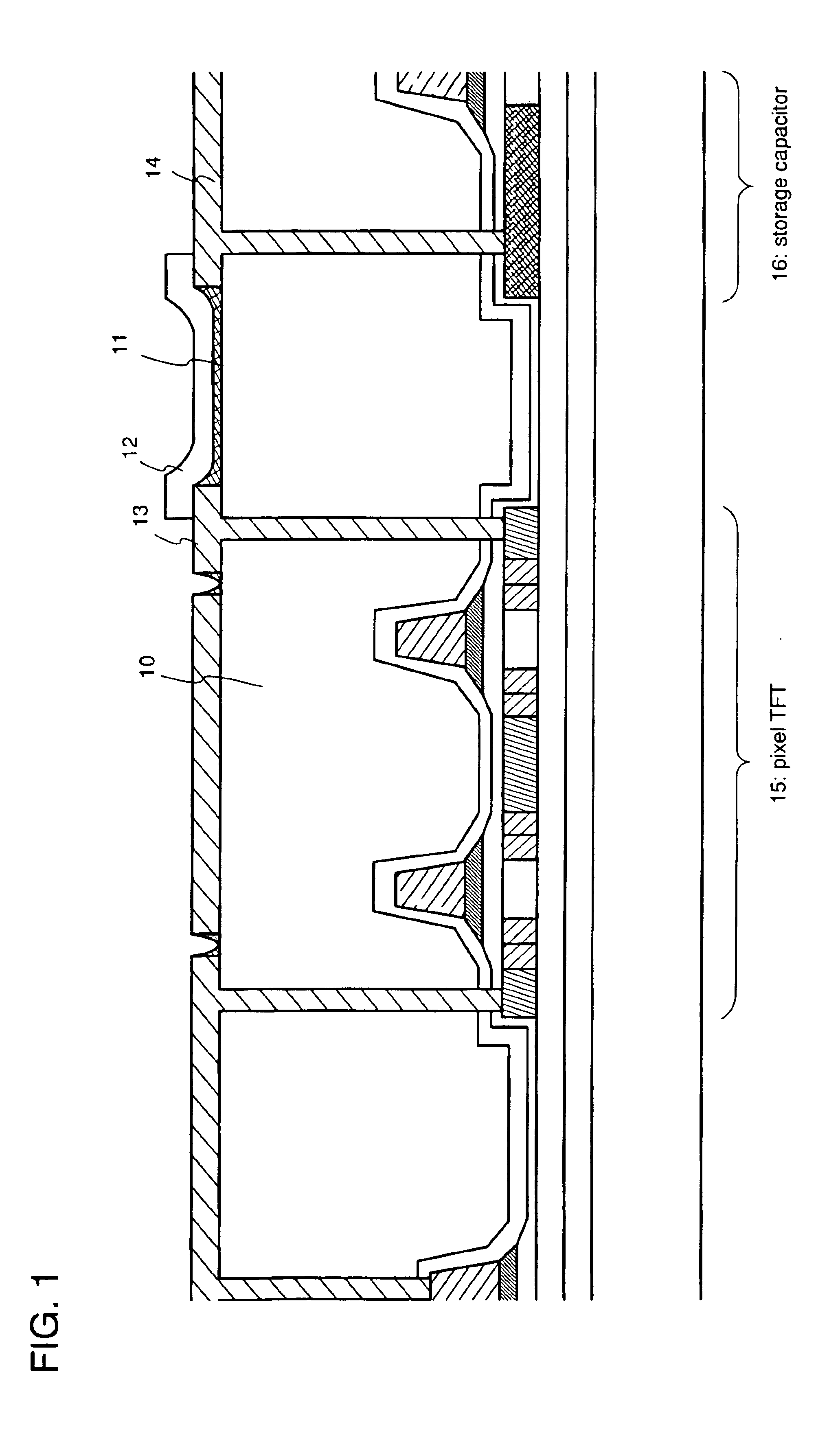
[0041]FIG. 1 shows a semiconductor device of the present invention. According to the present invention, in order to eliminate the disconnection of a pixel electrode 12 caused by a change in shape of an interlayer insulating film 10 at the ends of metal wiring, an insulating film (typically a resin film) 11 is formed on the interlayer insulating film 10. Specifically, the insulating film 11 is formed in a side portion of the metal wiring 13 and 14, which is interposed between the entire surface or a partial surface of the interlayer insulating film 10 and the pixel electrode 12 and has a curved surface at a portion (sidewall portion of the metal wiring) in contact with the metal wiring 13, 14, whereby the step difference of the ends of the metal wiring 13, 14 is alleviated. Thus, even if the interlayer insulating film 10 is changed in shape, the ends of the metal wiring 13, 14 are prevented from peeling, whereby the disconnection of the pixel electrode 12 can be pr...

embodiment mode 2

[Embodiment Mode 2]

[0048]Embodiment Mode 2 will be described with reference to FIGS. 15A to 15D. In Embodiment Mode 2, the shape of an insulating film (typically a resin film) formed so as to alleviate the step difference between the interlayer insulating film and the ends of metal wiring, described in Embodiment Mode 1, will be described. In FIGS. 15A to 15D, description will be made by using the same reference numerals as those in FIG. 1 used for description in Embodiment Mode 1.

[0049]FIG. 15A is a view showing the semiconductor device in FIG. 1, and FIGS. 15B to 15D are enlarged views illustrating an interlayer insulating film 10, metal wiring 13, 14, insulating films 11b to 11d (resin films are used in the present embodiment) that alleviate the step difference between the metal wiring and the interlayer insulating film, and a pixel electrode 12.

[0050]In FIG. 15B, the resin film 11b covers the side surface of the metal wiring 13 or 14 and a part of the surface of the interlayer i...

embodiments

[Embodiment 1]

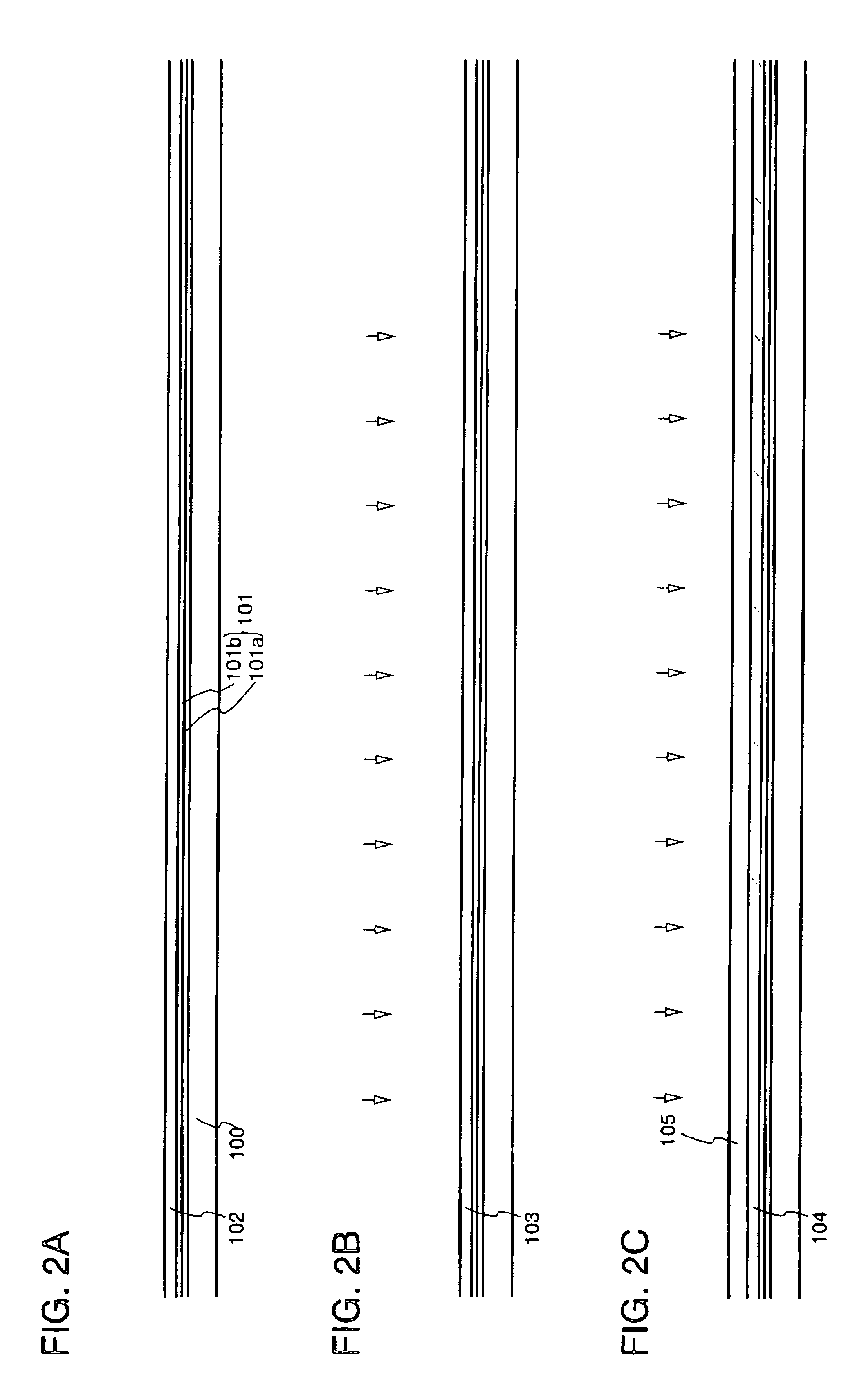
[0053]A method of manufacturing a semiconductor device adopting the present invention will be described with reference to FIGS. 2A-7B and FIG. 12.

[0054]First, FIG. 12 shows a circuit configuration of the entire semiconductor device adopting the present invention. The semiconductor display device is composed of a pixel region 1301, a gate signal line driving circuit 1312, and a source signal line driving circuit 1313. The gate signal line driving circuit 1312 includes a shift register circuit 1306, a level shifter circuit 1307, a buffer circuit 1308, a first protection circuit 1311, and a second protection circuit 1309. The source signal line driving circuit 1313 includes a shift register circuit 1302, a level shifter circuit 1303, a buffer circuit 1304, a sampling circuit 1305, and a precharge circuit 1310.

[0055]A method of manufacturing a semiconductor device with the above-described circuit configuration will be described specifically with reference to FIGS. 2A-7B.

[0...


PUM

PropertyMeasurementUnit
thicknessaaaaaaaaaa
thicknessaaaaaaaaaa
thicknessaaaaaaaaaa

Abstract

In order to eliminate the disconnection of a pixel electrode caused by a change in shape of an interlayer insulating film at the ends of metal wiring, a resin film is formed at the ends of the metal wiring. Because of the resin film at the ends of the metal wiring, the step difference of the ends of the metal wiring is alleviated, and even if the interlayer insulating film is changed in shape, the ends of the metal wiring is prevented from peeling, whereby the disconnection of the pixel electrode can be prevented. Furthermore, the resin film flattens the surface of the interlayer insulating film, and prevents an alignment defect of liquid crystal molecules and a non-uniform electric field, thereby suppressing a minute defect of a light-emitting device caused by the roughness of the surface of the pixel electrode.

Description

CROSS-REFERENCE TO RELATED APPLICATION[0001]This application is a divisional application of U.S. application Ser. No. 10 / 199,506, filed on Jul. 22, 2002 now U.S. Pat. No. 6,686,605, which claims the benefit of a foreign priority application filed in Japan on Jul. 27, 2001 as Ser. No. 2001-228164. This application claims priority to each of these prior applications, and the disclosures of the prior applications are considered part of (and are incorporated by reference in) the disclosure of this application.BACKGROUND OF THE INVENTION[0002]1. Field of the Invention[0003]The present invention relates to a semiconductor device having a circuit composed of thin film transistors (hereinafter referred to as TFTs), a display device such as a light emitting device and a liquid crystal display device, and a manufacturing method of the same. Specifically, the present invention relates to the technique of pixel electrode periphery portion structures.[0004]2. Description of the Related Art[0005]...

Claims


Application Information

Patent Timeline
Patent Type & Authority Patents(United States)
IPC IPC(8): G02F1/13G02F1/1362H01L21/70H01L27/12H01L21/84G02F1/1368G09F9/30H01L21/20H01L21/768H01L21/77H01L29/786
CPCG02F1/136227H01L27/12H01L27/1248G02F1/136213
Inventor SAKAKURA, MASAYUKIMURAKAMI, SATOSHIYAMAGATA, HIROKAZU
Owner SEMICON ENERGY LAB CO LTD
Learn More