Method of forming grating microstructures by anodic oxidation

a microstructure and oxidation technology, applied in the direction of diffraction gratings, instruments, electrical appliances, etc., can solve the problems of disadvantageous differences between the duty ratios of the upper and lower portions of the grating groove pattern and each other, disadvantageous differences in the duty ratio of the upper and lower portions of the grating groove pattern and the optical element having excellent birefringence property, etc., to achieve the effect of excellent grating groove patterns

Inactive Publication Date: 2005-08-16
SANYO ELECTRIC CO LTD
View PDF2 Cites 15 Cited by
  • Summary
  • Abstract
  • Description
  • Claims
  • Application Information

AI Technical Summary

Benefits of technology

[0021]In the method of manufacturing an element having a microstructure according to the first aspect, the surface of the metal layer formed with the dot column of concave portions is anodically oxidized in the state opposed to the cathode surface as hereinabove described, whereby the linear grating groove pattern having a large depth with a uniform groove width along the depth direction can be easily formed in a self-organized manner when the interval between the concave portions of the dot column is reduced. Consequently, an element having a microstructure of an excellent grating groove pattern or the like can be easily formed. When the method of manufacturing an element according to the first aspect is applied to formation of an optical element serving as an exemplary element having a microstructure in this case, an optical element having an excellent birefringence property can be easily formed.
[0054]In the element having a microstructure according to the seventh aspect, the metal oxide film having a rectilinear grating groove pattern is formed on the substrate as hereinabove described, whereby the rectilinear grating groove pattern having a large depth with a uniform groove width along the depth direction can be easily formed in a self-organized manner when the metal oxide film is formed by anodic oxidation, so that an element having a microstructure of an excellent rectilinear grating groove pattern or the like can be easily obtained. When the structure according to the seventh aspect is applied to an optical element serving as an exemplary element having a microstructure, an optical element having an excellent birefringence property can be easily obtained.

Problems solved by technology

In the case of forming the rectilinear grating groove patterns of the conventional wave plate 100 shown in FIG. 45 or the rectilinear grating groove patterns 100a and 100b of the conventional polarization-dependent diffraction grating shown in FIG. 47 by photolithography and etching, however, it is difficult to form grating groove patterns having a large depth with a uniform groove width along the depth direction.
More specifically, rectilinear grating groove patterns deeply formed by photolithography and etching have trapezoidal sections non-uniform in the depth direction as shown in FIG. 48, and hence duty ratios in upper and lower portions of the grating groove patterns disadvantageously differ from each other.
Consequently, it is difficult to form an element having a microstructure of excellent grating groove patterns or the like, and hence it is disadvantageously difficult to obtain an optical element having an excellent birefringence property.
As hereinabove described, it has been difficult to form a linear grating groove pattern having a large depth with a uniform groove width along the depth direction in general, and hence it has been difficult to form an element having a microstructure of an excellent grating groove pattern or the like.

Method used


Image

  • Method of forming grating microstructures by anodic oxidation
  • Method of forming grating microstructures by anodic oxidation
  • Method of forming grating microstructures by anodic oxidation

Examples


first embodiment

[0092](First Embodiment)

[0093]A process of manufacturing a wave plate according to a first embodiment of the present invention is described with reference to FIGS. 1 to 7.

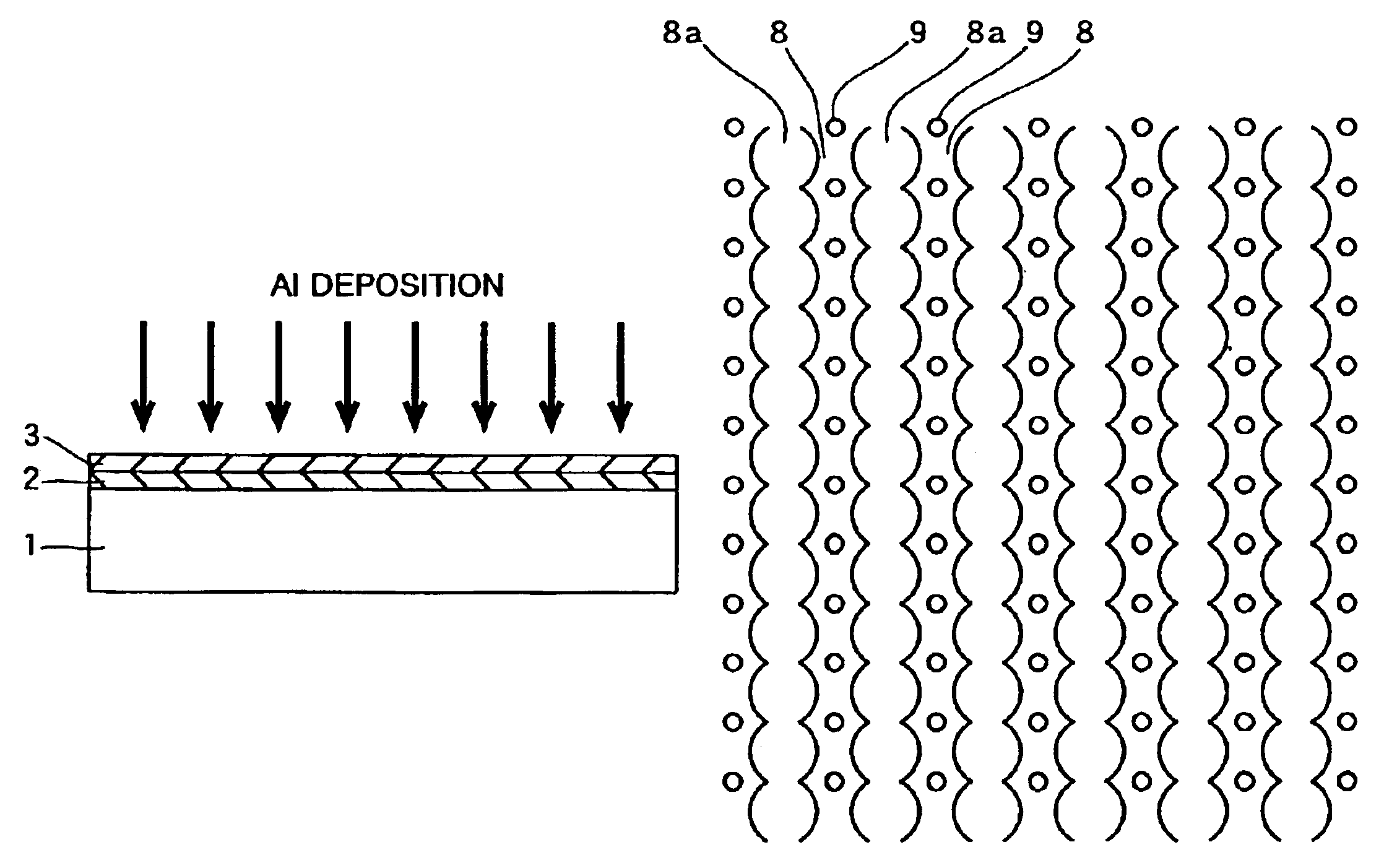
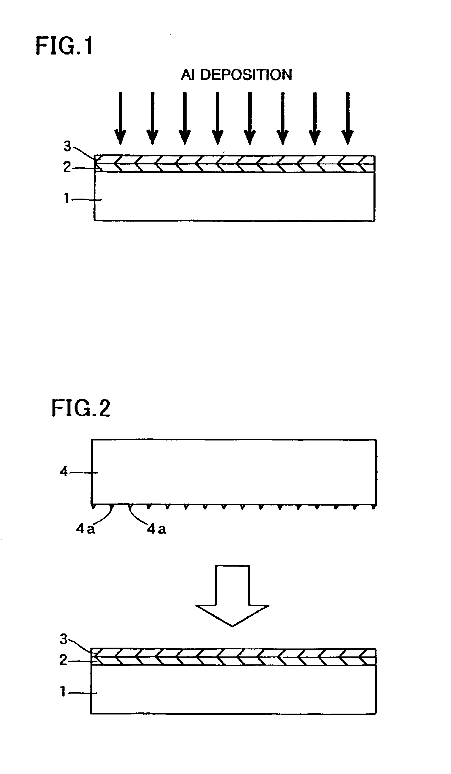
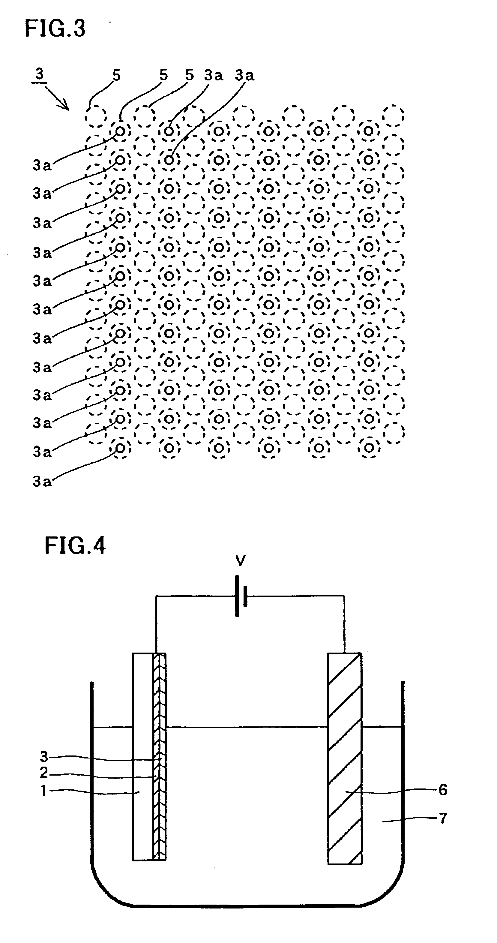
[0094]First, a transparent electrode film 2 consisting of ITO or ZnO and an aluminum film 3 having a thickness of about 3 μm are successively formed on a glass substrate 1 by vapor deposition, as shown in FIG. 1. The glass substrate 1 is an example of the “substrate” in the present invention, and the transparent electrode film 2 is an example of the “transparent conductor film” in the present invention. The aluminum film 3 is an example of the “metal layer” in the present invention.

[0095]As shown in FIG. 2, regularly arranged projecting portions 4a are formed on the surface of a press member 4 consisting of a hard material such as SiC, in order to perform texturing. According to the first embodiment, the projecting portions 4a (see FIG. 2) of the press member 4 are so formed as to define dot columns of concave port...

second embodiment

[0103](Second Embodiment)

[0104]Referring to FIGS. 10 to 12, a manufacturing process according to a second embodiment of the present invention is similar to that according to the aforementioned first embodiment except that positions of dot columns of concave portions 13a formed on an aluminum film 13 by texturing are different from those in the first embodiment.

[0105]In the manufacturing process according to the second embodiment, texturing is so performed as to form the dot columns of the concave portions 13a on the surface of the textured aluminum film 13 every other column of triangular lattice patterns 5 arranged in a plurality of columns shown by broken lines while alternating adjacent ones of the dot columns of the concave portions 13a, as shown in FIG. 10. Thus, the dot columns of the concave portions 13a are formed on the surface of the aluminum film 13 in the arrangement shown in FIG. 10. The aluminum film 13 is an example of the “metal layer” in the present invention.

[0106]...

third embodiment

[0108](Third Embodiment)

[0109]Referring to FIGS. 13 to 15, grating groove patterns are formed by rectilinearly coupling a larger number of micropores with each other in a manufacturing process according to a third embodiment of the present invention as compared with the aforementioned first and second embodiments.

[0110]In the process of manufacturing the grating groove patterns of a wave plate according to the third embodiment, positions of dot columns of concave portions 23a formed on an aluminum film 23 by texturing are different from those in the aforementioned first and second embodiments, as shown in FIG. 13. More specifically, texturing is so performed as to form the dot columns of the concave portions 23a every other column of triangular lattice patterns 5 arranged in a plurality of columns shown by broken lines so that the interval along the column direction is narrower than the interval between the triangular lattice patterns 5. The aluminum film 23 is an example of the “me...


PUM

PropertyMeasurementUnit
refractive indicesaaaaaaaaaa
depthaaaaaaaaaa
thicknessaaaaaaaaaa

Abstract

A method of manufacturing an element having a microstructure of an excellent grating groove pattern or the like is obtained. This method of manufacturing an element having a microstructure comprises steps of forming a metal layer on a substrate, forming a dot column of concave portions on the surface of the metal layer and anodically oxidizing the surface of the metal layer formed with the dot column of concave portions while opposing this surface to a cathode surface thereby forming a metal oxide film having a grating groove pattern. When the interval between the concave portions of the dot column is reduced, therefore, a linear grating groove pattern having a large depth with a uniform groove width along the depth direction is easily formed in a self-organized manner.

Description

BACKGROUND OF THE INVENTION[0001]1. Field of the Invention[0002]The present invention relates to an element having a microstructure and a method of manufacturing the same, and more particularly, it relates to an element having a microstructure formed by anodic oxidation and a method of manufacturing the same.[0003]2. Description of the Background Art[0004]In general, a method employing photolithography and etching or a method employing anodic oxidation is known as a method of manufacturing a microstructure of a micro lattice pattern or the like. In recent years, an element having a micro grating groove pattern such as an optical element has been implemented through photolithography and etching.[0005]FIG. 45 is a perspective view showing the concept of a conventional wave plate (polarization element) 100 serving as an element having a microstructure. In the conventional wave plate 100, groove patterns constituting a grating are formed on a glass substrate 101, as shown in FIG. 45. Th...

Claims


Application Information

Patent Timeline
Patent Type & Authority Patents(United States)
IPC IPC(8): G02B5/18
CPCG02B5/1809G02B5/1857
Inventor MORI, KAZUSHIMATSUMOTO, MITSUAKITOMINAGA, KOJITAJIRI, ATSUSHIFURUSAWA, KOUTAROU
Owner SANYO ELECTRIC CO LTD
Why Eureka
Try Eureka