[0009]Embodiments of the present invention solve these problems by ensuring that the MTJ's have a minimized
voltage drop across the MTJ's, for both selected cells and non-selected cells, during a write operation. The direction of the
write current for a word line and
bit line of a selected MTJ is chosen according to the physical location of the selected MTJ in the array, to reduce the
voltage drop across the selected MTJ. In one embodiment, the word lines of non-selected MTJ's are coupled to a mid-point voltage of the selected MTJ bit lines, and the bit lines of non-selected MTJ's are coupled to a mid-point voltage of the selected MTJ word lines, during the write operation of selected MTJ'S. In another embodiment, a resistance is added to each
bit line or word line of non-selected MTJ's, to eliminate the
voltage drop across the non-selected MTJ's.
[0010]In accordance with a preferred embodiment of the present invention, a method of storing information to a magnetic memory device includes providing a cross-point magnetic
memory cell array, the array including a plurality of first conductive lines running parallel to one another in a first direction, a plurality of second conductive lines running parallel to one another in a second direction, the second direction being different from the first direction, and a plurality of MTJ's disposed between the first conductive lines and the second conductive lines at the intersections of the first conductive lines and the second conductive lines. The method includes selecting at least one MTJ to store information in, wherein the other MTJ's are unselected, and storing information in the selected at least one MTJ by running a first current through the first conductive line of the selected at least one MTJ while running a second current through the second conductive line of the selected at least one MTJ and while minimizing a voltage drop across at least one of the MTJ's.
[0012]In accordance with yet another preferred embodiment of the present invention, a method of minimizing a voltage drop across at least one selected MTJ during a write operation in a cross-point magnetic
memory cell array including a plurality of first conductive lines running parallel to one another in a first direction, a plurality of second conductive lines running parallel to one another in a second direction, the second direction being different from the first direction, and a plurality of MTJ's being disposed between the first conductive lines and the second conductive lines at the intersections of the first conductive lines and the second conductive lines, a
current source / drain (CSD) being coupled to an end of each first conductive line and each second conductive line, each CSD being adapted to function as a
current source or a current drain. The method includes storing information in the selected at least one MTJ by running a first current from a CSD at a first end of the first conductive line to a CSD at a second end of the first conductive line of the selected at least one MTJ while running a second current from a CSD at a first end of the second conductive line to a CSD at a second end of the second conductive line of the selected at least one MTJ, wherein the direction of the first current and second current is selected as a function of the physical location of the at least one selected MTJ in the array to minimize the voltage drop of the at least one selected MTJ.
[0013]In accordance with another preferred embodiment of the present invention, a method of minimizing a voltage drop across unselected MTJ's during a write operation of at least one selected MTJ in a cross-point magnetic
memory cell array including a plurality of first conductive lines running parallel to one another in a first direction, a plurality of second conductive lines running parallel to one another in a second direction, the second direction being different from the first direction, and a plurality of MTJ's being disposed between the first conductive lines and the second conductive lines at the intersections of the first conductive lines and the second conductive lines, a CSD being coupled to an end of each first conductive line and each second conductive line, each CSD being adapted to function as a
current source or a current drain, the cross-point memory
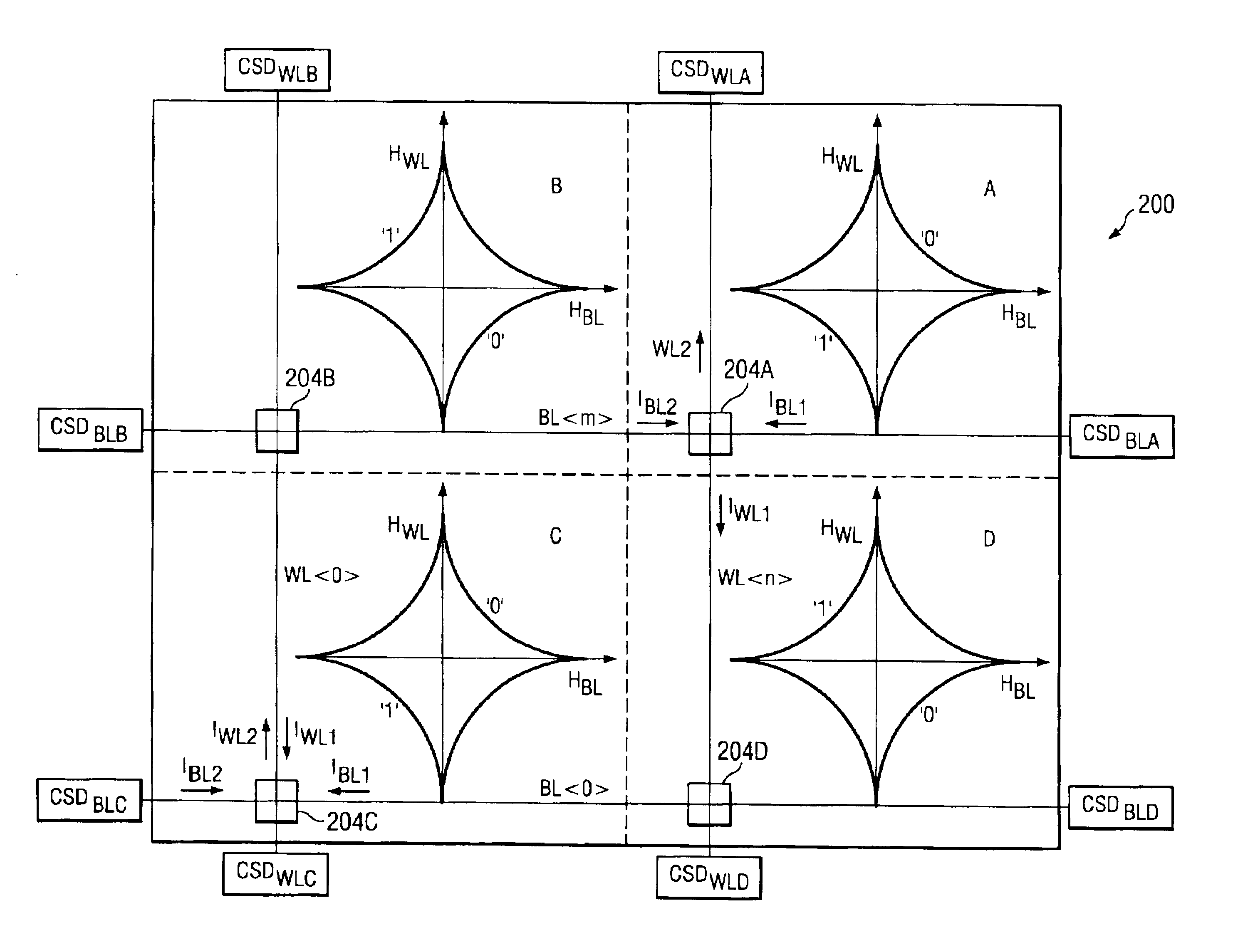
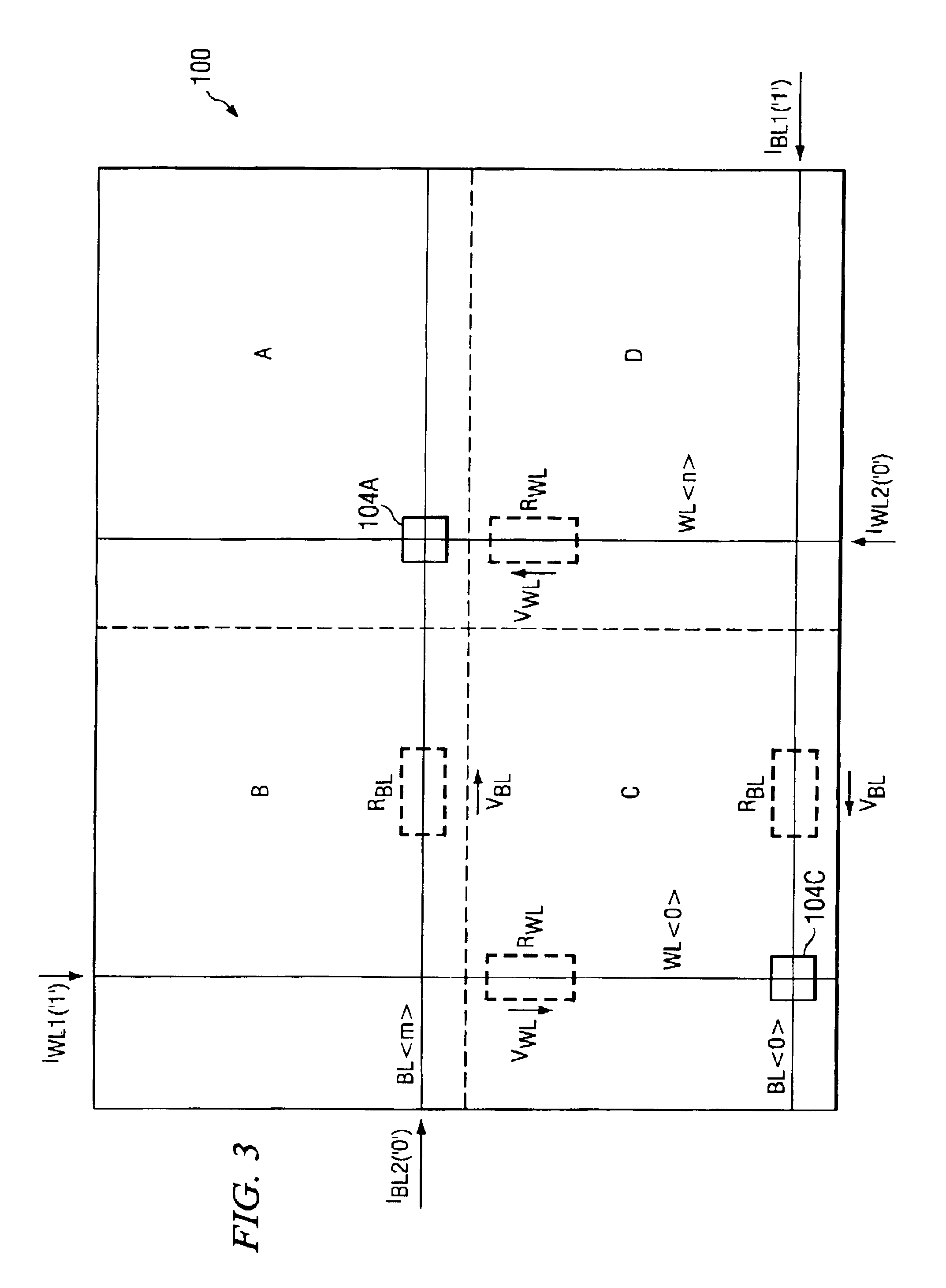
cell array having a top edge, a bottom edge, a left edge and a right edge. The method includes storing information in the selected at least one MTJ by running a first current from a CSD at a first end of the first conductive line to a CSD at a second end of the first conductive line of the selected at least one MTJ while running a second current from a CSD at a first end of the second conductive line to a CSD at a second end of the second conductive line of the selected at least one MTJ, wherein the voltage drop across the unselected magnetic tunnel junctions is minimized by clamping the first conductive lines or second conductive lines of the unselected MTJ's to a mid-point voltage.
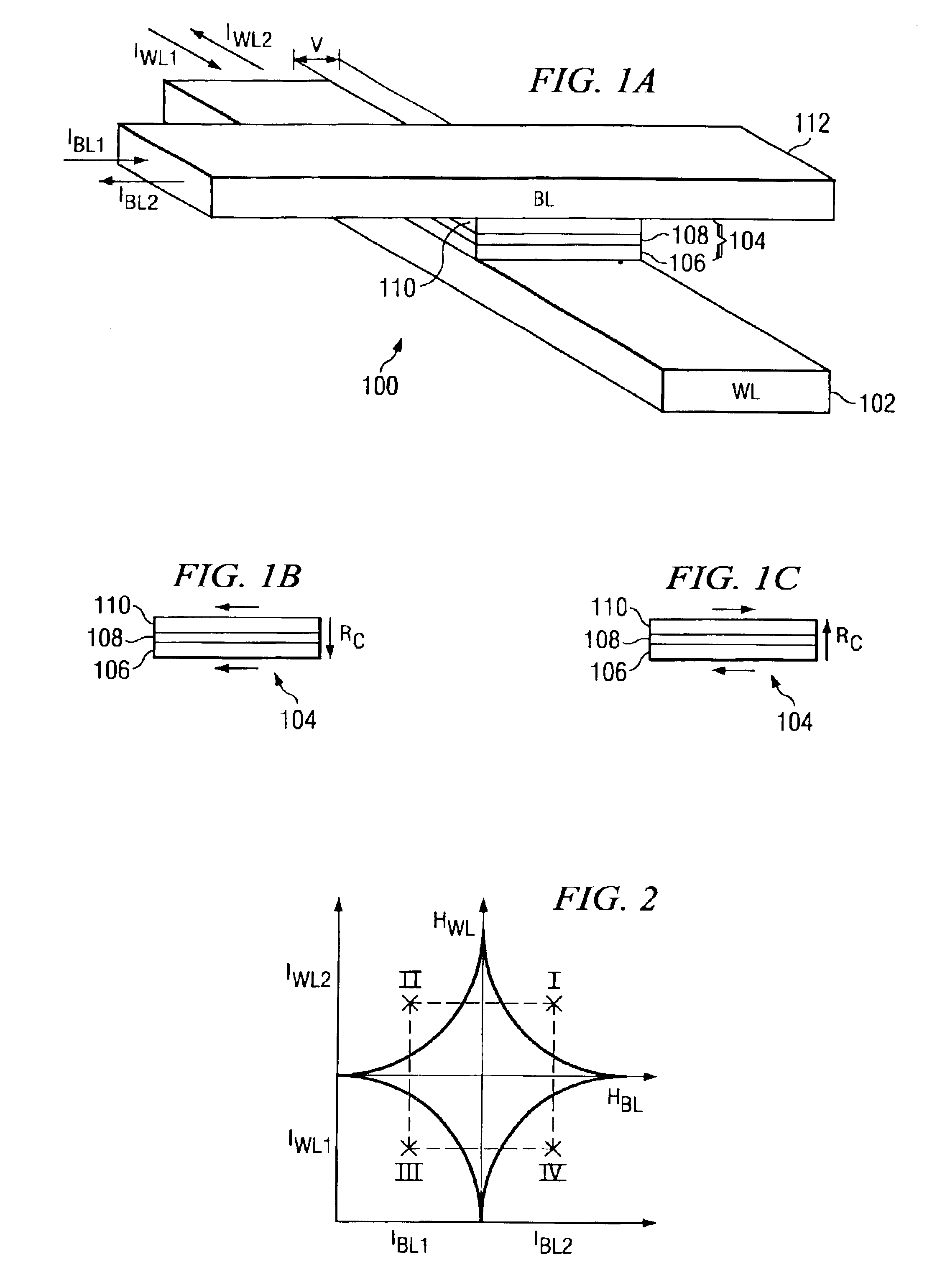
[0014]Advantages of minimizing the voltage drop of selected MTJ's in accordance with embodiments of the present invention include achieving a decreased maximum voltage across the selected MTJ during the write operation. Because the voltage drop is reduced or minimized, less damage to MTJ's results. The full range, e.g., all quadrants, of the
asteroid curve of the MTJ
cell is advantageously utilized in a novel way, by changing the direction of the current on both the bit lines and word lines in a write operation.
[0015]Advantages of minimizing the voltage drop of non-selected MTJ's include decreasing the leakage current through the selected MTJ's during the write operation. The
write margin is increased due to minimized leakage current along the selected word line and
bit line. Adding resistance to the edge of the word lines or bit lines results in all unselected MTJ's being clamped to the same voltage, which means that there is no stress on the MTJ's and no parasitic currents through the unselected MTJ's, decreasing
power consumption and increasing
write margin.

