Optical scan module, optical scanner, optical scan method, image generator and image reader

Inactive Publication Date: 2005-08-23
RICOH KK
View PDF42 Cites 46 Cited by
  • Summary
  • Abstract
  • Description
  • Claims
  • Application Information

AI Technical Summary

Benefits of technology

[0020]It is an object of the present invention to provide an optical scan module that can constitute a high-precision optical scanner with ease in accordance with the

Problems solved by technology

However, these publications have failed to disclose a concept of making a module of a single integral optical scan unit associated with a standard size paper sheet, nor a mounting unit for mounting to another member.
However, these publications have failed to disclose a mounting unit for mounting a plurality of optical scan unit to another member.
Although an object is proposed to render a joint part of scan lines unobtrusive when a single scan line is divided to be simultaneously scanned with two light beams, it is difficult to grasp as a clear concrete measure for solution.
In the electronic photographic image generator having an optical scanner as described, if a vibration of a body of the electronic photogr

Method used


Image

  • Optical scan module, optical scanner, optical scan method, image generator and image reader
  • Optical scan module, optical scanner, optical scan method, image generator and image reader
  • Optical scan module, optical scanner, optical scan method, image generator and image reader

Examples


first embodiment

[0067]The first embodiment relates to the optical scan module according to this invention.

[1-a] First Aspect of the First Embodiment

[0068]A first example of the first aspect of the first embodiment will be explained here.

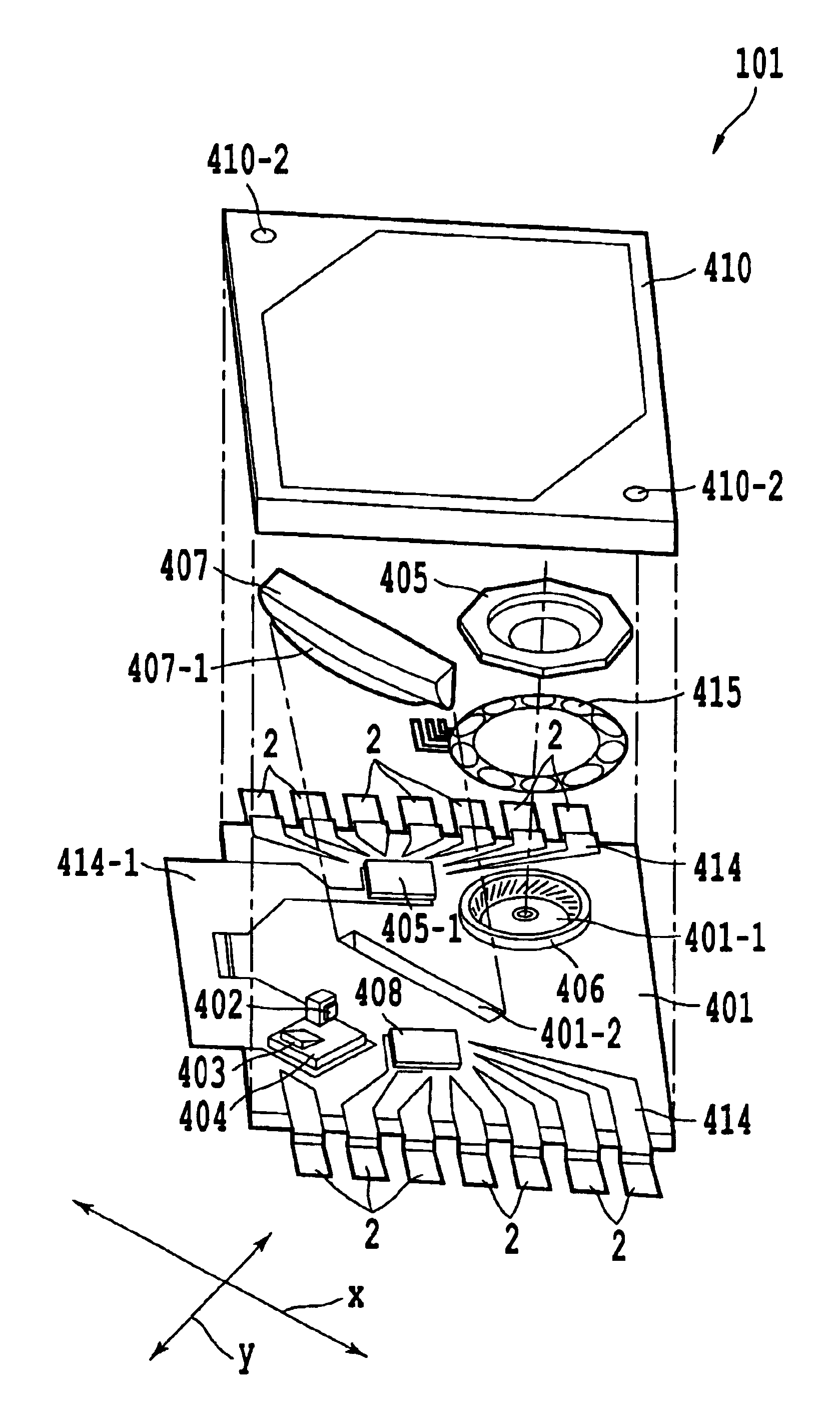
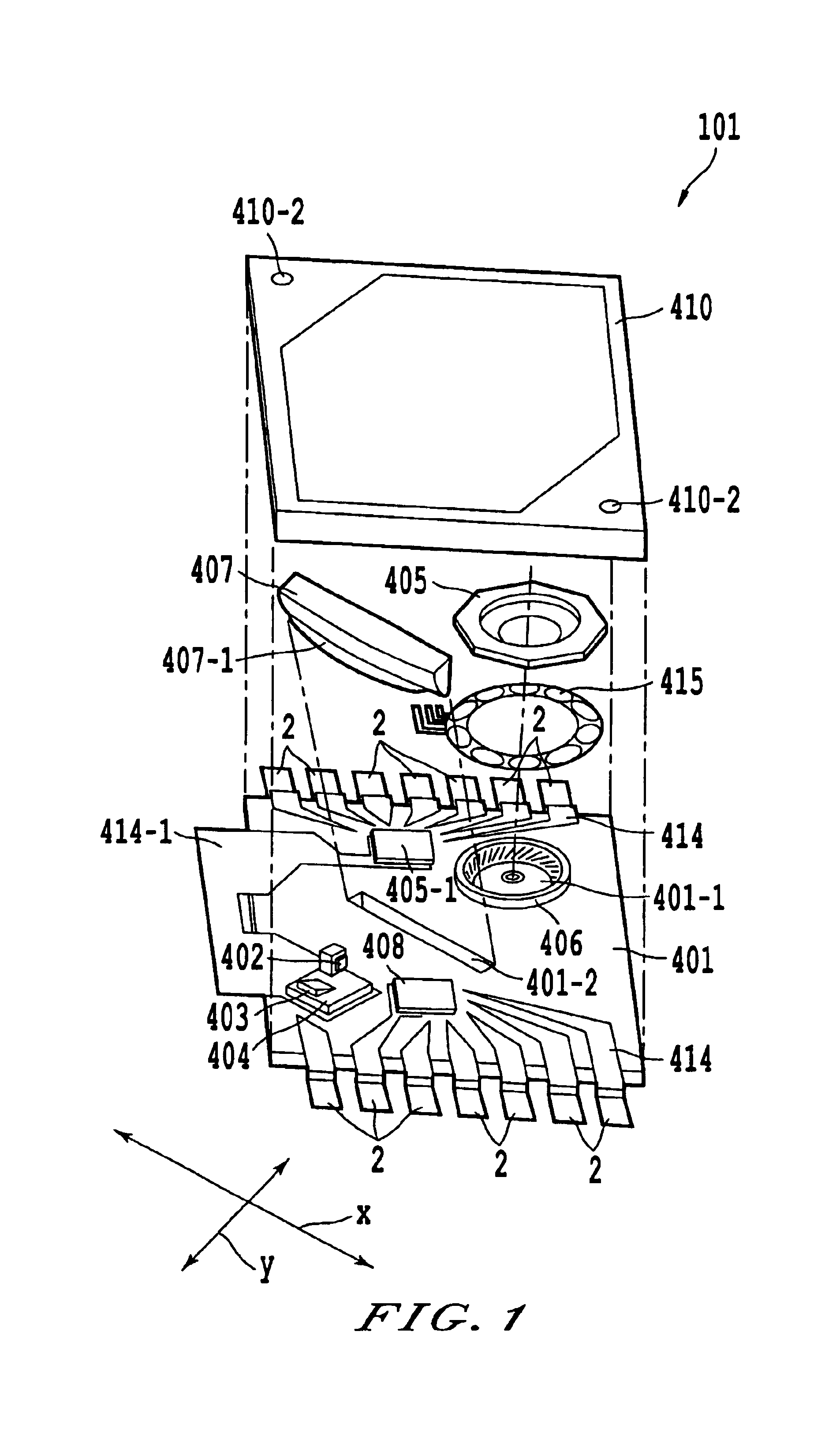
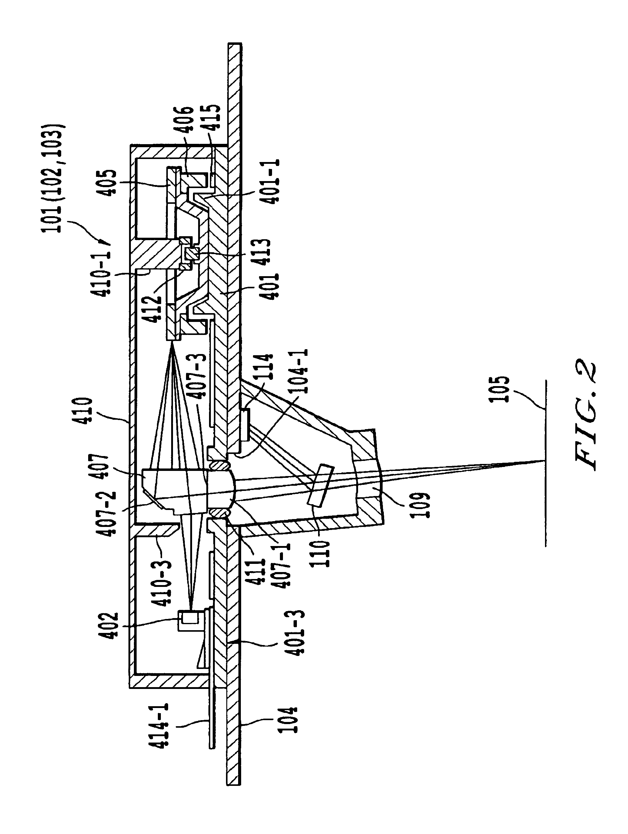
[0069]FIG. 1 shows an exploded state of an optical scan module 101 according to this example, and FIG. 2 shows a section of the optical scan module 101 in an assembled state. In these figures, designated by reference character 401 is a ceramic substrate molded in a rectangular plate form, as an electrode substrate having electrodes such as terminals and as an electrode substrate holding various members.

[0070]The electrode substrate 401 has integrally applied thereon an LD (laser diode, as used herein) chip 402 as a light emission source, a photo diode 403 joined to an LD mount 404 for monitoring a light quantity, a drive circuit formed on a bare chip 408 for use to the light emission source, a drive circuit formed on a bare chip 405-1 for use to a deflection unit, a...

second embodiment

[0208]The second embodiment will be explained now. This embodiment covers examples in which the above-noted optical scan module is mounted on another member, for example on a circuit substrate, to constitute the optical scanner according to this invention.

[0209]A first example of the second embodiment will be explained here.

[0210]FIG. 12 shows an example of an optical scanner 1 constituted with a combination of k=3 optical scan modules 101 described with reference to FIG. 1 and FIG. 2. FIG. 2 shows a section of an optical scan module 101 in FIG. 1. The optical scan module 101 of FIG. 1 and FIG. 2 and optical scan modules 102 and 103 quite identical to the optical scan module 101 are arrayed along a principal scan direction X, and applied on a circuit substrate 104, with a matching scan direction, to provide the example. In FIG. 12, the optical scan modules 101, 102, and 103 are depicted as they are seen through their caps 410 shown in FIG. 1.

[0211]The optical scan modules 101, 102, ...

third embodiment

[0237]The third embodiment will be explained now. This embodiment is principally addressed to the optical scanner this invention.

[0238]In usual system in which a deflector is used for scanning a light beam to record an image, a distance from the deflector to a surface to be scanned increases in proportion to the dimension of a record width, resulting in an enlarged apparatus scale that needs the aperture of a scan lens as well as a deflector to be enlarged, as a disadvantage. To the contrary, as described, compact design can be achieved by arranging a plurality of optical scan modules on a common circuit substrate, and dividing a total record width to be scanned. Moreover, the record width can be increased by simply changing the number of optical scan modules to be joined together, without increasing the distance to a surface to be scanned.

[0239]However, at a respective optical scan module, there is recorded an image data of a division of one line. Because deflection unit are asynch...


PUM


Abstract

An optical scanning apparatus scans a surface to be scanned in a main scanning direction by simultaneously using a plurality of optical spots formed of a plurality of optical beans emitted from an illuminant, comprising: a light path deflecting part deflecting a light path of at least one of the optical beams, wherein the light path deflecting part is provided in light paths of the optical beams wherein the light path deflecting part may use a liquid crystal deflecting element formed of a liquid crystal element being controllable by an electronic signal to deflect the light path of the one of the optical beams.

Description

FIELD OF THE INVENTION[0001]The present invention in general relates to an optical scan module, an optical scanner, an optical scan method, an image generator, and an image reader.BACKGROUND OF THE INVENTION[0002]The following publications disclose the techniques relating to an optical scan unit constituted as a single integral body with a function for deflecting a light beam from a light emission source by a deflection unit to repeat scanning. That is,[0003]a) Japanese Patent Application Laid-Open Publication No. 4-96014,[0004]b) Japanese Patent Application Laid-Open Publication No. 4-328715,[0005]c) Japanese Patent Application Laid-Open Publication No. 6-3613,[0006]d) Japanese Patent Application Laid-Open Publication No. 9-146129,[0007]e) Japanese Patent Publication No. 2668725, and[0008]f) Japanese Patent Publication No. 2722630.However, these publications have failed to disclose a concept of making a module of a single integral optical scan unit associated with a standard size p...

Claims


Application Information

Patent Timeline
IPC IPC(8): G06K15/12
CPCG06K7/1098G06K15/1204
Inventor NAKAJIMA, TOMOHIROITABASHI, AKIHISA
Owner RICOH KK
Why Eureka
Try Eureka