Unlock instant, AI-driven research and patent intelligence for your innovation.

ESD protection apparatus and method for dual-polarity input pad

a protection apparatus and input pad technology, applied in emergency protection circuit arrangements, transistors, etc., can solve the problem of large chip area of charge-pumping circuits

Inactive Publication Date: 2005-08-23
MACRONIX INT CO LTD
View PDF3 Cites 25 Cited by
  • Summary
  • Abstract
  • Description
  • Claims
  • Application Information

AI Technical Summary

Benefits of technology

[0005]An ESD protection apparatus and method for dual-polarity input pad, according to the present invention, comprises formation of a silicon controlled rectifier (SCR) structure on a semiconductor substrate, which includes two semiconductor regions of first conductivity type inserted with another semiconductor region of second conductivity type opposite to the first conductivity type therebetween, preferably in the manner of a triple-well made by complementary metal-oxide semiconductor (CMOS) process. On the two semiconductor regions of the first conductivity type, a first and a second electrode connection regions of opposite conductivity types are formed and connected to the input pad and ground pad, respectively. A further region of the second conductivity type bridges across the semiconductor region of the second conductivity type betwee

Problems solved by technology

However, the charge-pumping circuit occupies large chip area.
Unfortunately, the negative supply voltage may be high up to −7V depending on the programming / erasing for various applications.

Method used


Image

  • ESD protection apparatus and method for dual-polarity input pad
  • ESD protection apparatus and method for dual-polarity input pad
  • ESD protection apparatus and method for dual-polarity input pad

Examples


Embodiment Construction

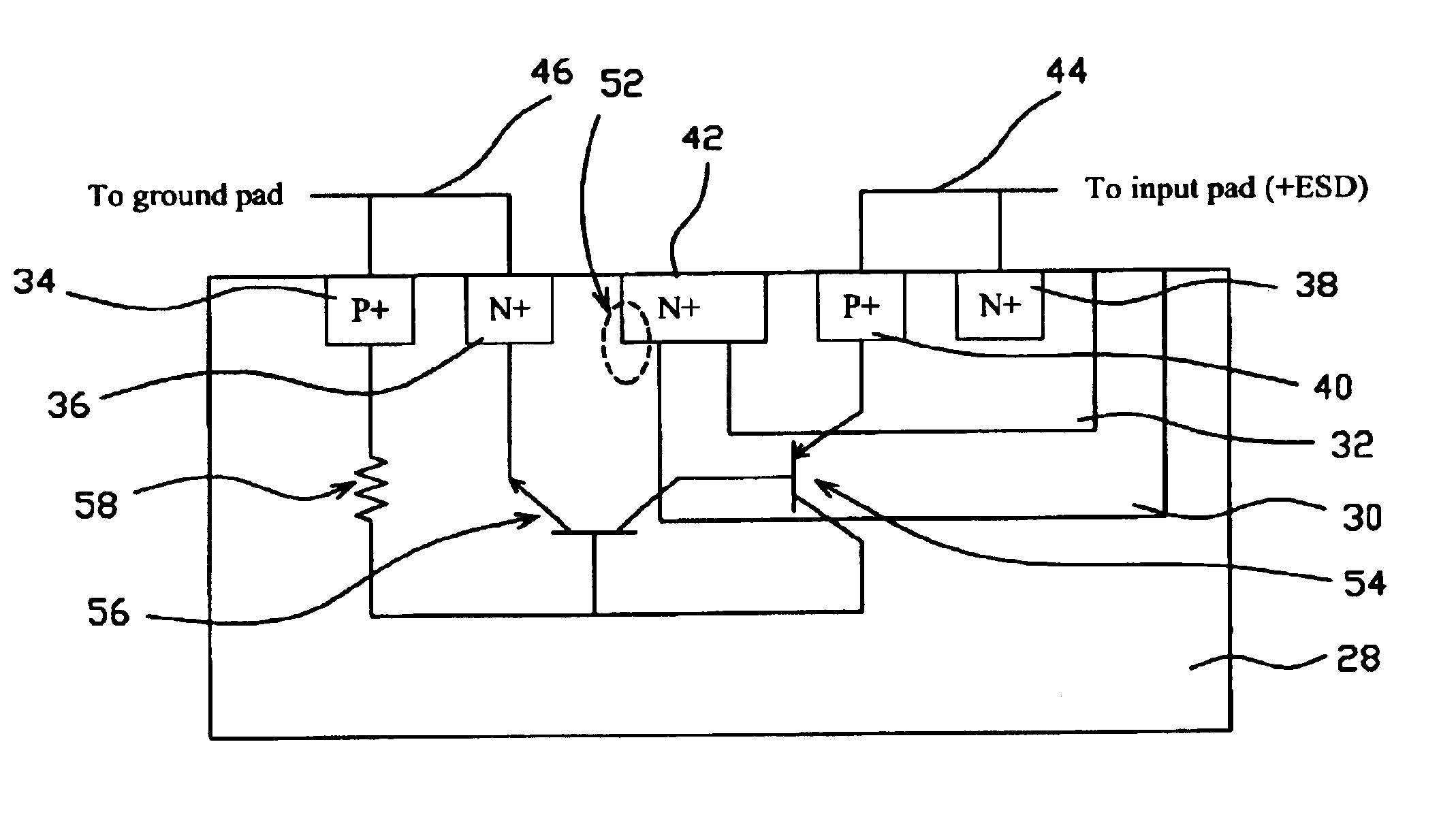
[0015]FIG. 2 is a preferred embodiment of the present invention. A deeper N-type well 30 is formed in a P-type substrate or well 28, and a P-type well 32 is further formed in the N-type well 30. Hence, the P-type substrate or well 28, N-type well 30, and P-type well 32 form a triple-well structure, which can be obtained by CMOS process. A ground connection region 29 is formed on the P-type substrate or well 28, which includes P+ region 34 and N+ region 36 both connected to a ground pad 46. An input connection region 31 is formed on the P-type well 32, which includes N+ region 38 and P-type region 40 both connected to an input pad 44. An N+ region 42 is formed across the N-type well 30 and extends to the P-type substrate or well 28 and P-type well 32.

[0016]As shown in FIG. 3, under normal operation, there will be formed, in the apparatus of FIG. 2 by the P-type substrate or well 28, N-type well 30 and P-type well 32, two parasitic diodes 48 and 50 back-to-back connected between the g...


PUM


Abstract

An ESD protection apparatus for dual-polarity input pad comprises a triple-well formed with a first, second and third regions to form an SCR structure. A first and second ground connection regions of opposite conductivity types are formed on the first region, a first and second input connection regions of opposite conductivity types are formed in the third region, and a bridge region is formed across the second region and extends to the first and third regions. Under normal operation, the first, second, and third regions form two back-to-back diodes. Under positive polarity ESD event, breakdown is occurred between the bridge and first regions to thereby trigger an SCR circuit for positive polarity ESD protection. Under negative polarity ESD event, breakdown is occurred between the bridge and third regions to thereby trigger an SCR circuit for negative polarity ESD protection.

Description

FIELD OF THE INVENTION[0001]The present invention relates generally to an electro-static discharge (ESD) protection apparatus and method, and more particularly to an ESD protection apparatus and method for dual-polarity input pad.BACKGROUND OF THE INVENTION[0002]In semiconductor memories, especially for erasable programmable read only memory (EPROM) and flash memory, some program / erase schemes thereof require negative supply voltages in addition to positive supply voltages. Typically, such negative voltages are supplied by use of charge-pumping circuits. However, the charge-pumping circuit occupies large chip area. To economize the area of silicon wafer, it is desired for circuit designers to have negative voltages supplied directly from appropriate pins during programming / erasing.[0003]On the other hand, N-type device formed in P-type substrate or well connected between input pad and ground pad is usually served as ESD protection apparatus with the P-type substrate or well grounded...

Claims


Application Information

Patent Timeline
IPC IPC(8): H01L27/02
CPCH01L27/0262H01L29/87
Inventor LIU, MENG-HUANGLAI, CHUN-HSIANGSU, SHINLU, TAO-CHENG
Owner MACRONIX INT CO LTD