Light emitting diode package with diffuser and method of manufacturing the same

a technology of led package and diffuser, which is applied in the direction of basic electric elements, electrical appliances, semiconductor devices, etc., can solve the problems of not being suitable for mass production, not necessarily allowing uniform light emission, and mediocre color reproducibility, so as to reduce the number of led package components, reduce the thickness of the lens part, and increase the degree of freedom

Active Publication Date: 2009-03-10
SAMSUNG ELECTRONICS CO LTD
View PDF8 Cites 432 Cited by
  • Summary
  • Abstract
  • Description
  • Claims
  • Application Information

AI Technical Summary

Benefits of technology

[0027]Another object of certain embodiments of the invention is to provide an LED package using a diffuser which emits light generated from an LED chip in a wide radiating angle without distortion of light, thereby increasing a degree of freedom and reducing a thickness of a lens part, and a manufacturing method of the same.
[0028]Further another object of certain embodiments of the invention is to provide an LED package using a diffuser which constitutes a Liquid Crystal Display (LCD) backlight unit in a fewer number, thereby decreasing the number of LED package components and reducing the manufacturing costs of the LCD backlight unit, and a manufacturing method of the same.
[0029]According to an aspect of the invention for realizing the object, there is provided a light emitting diode package including: a substrate with an electrode formed thereon; a light emitting diode chip mounted on the substrate; an encapsulant applied around the light emitting diode chip, the encapsulant containing a diffuser; and a lens part disposed on the light emitting diode chip and the encapsulant to radiate light in a wide angle, whereby light from the light emitting diode chip is emitted out of the package without distortion.
[0035]According to another aspect of the invention for realizing the object, there is provided a manufacturing method of a light emitting diode package including steps of: providing a substrate with an electrode formed thereon; mounting a light emitting diode chip on the substrate; applying an encapsulant containing a diffuser to cover the light emitting diode chip; and attaching a lens part on the encapsulant, whereby light from the light emitting diode chip is emitted out of the package without distortion.

Problems solved by technology

Although the conventional technology is useful for elongating the wavelength of light emitted from the LED chip 210 and emitting white light, it does not necessarily allow uniform light emission.
Further, as it realizes white light using the phosphor 222a, it has mediocre color reproducibility.
In addition, the conventional LED package 250 is complicated to manufacture, thus not suitable for mass production.
However, the conventional LED package 300 also emits light only forward from the molded frame 315, and does not achieve excellent light emission.
Therefore, the conventional LED packages 200, 250 and 300 result in increased manufacturing costs of the LCD products due to the increased number of components.

Method used


Image

  • Light emitting diode package with diffuser and method of manufacturing the same
  • Light emitting diode package with diffuser and method of manufacturing the same
  • Light emitting diode package with diffuser and method of manufacturing the same

Examples


Embodiment Construction

[0048]Preferred embodiments of the present invention will now be described in detail with reference to the accompanying drawings.

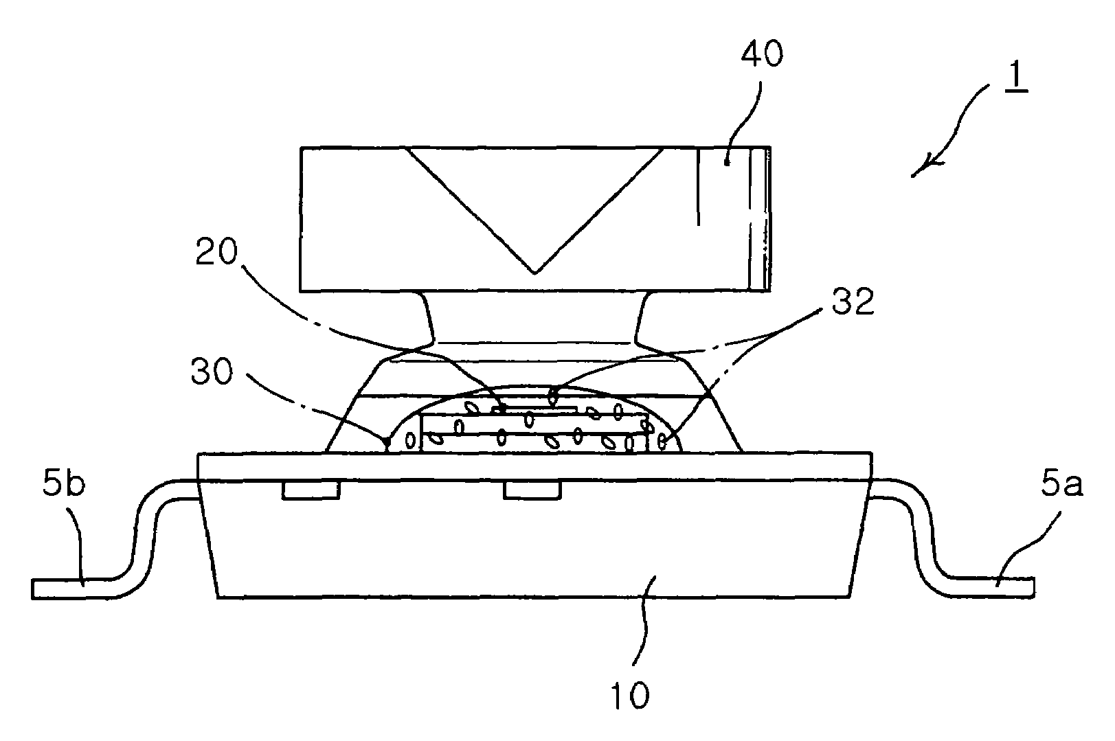
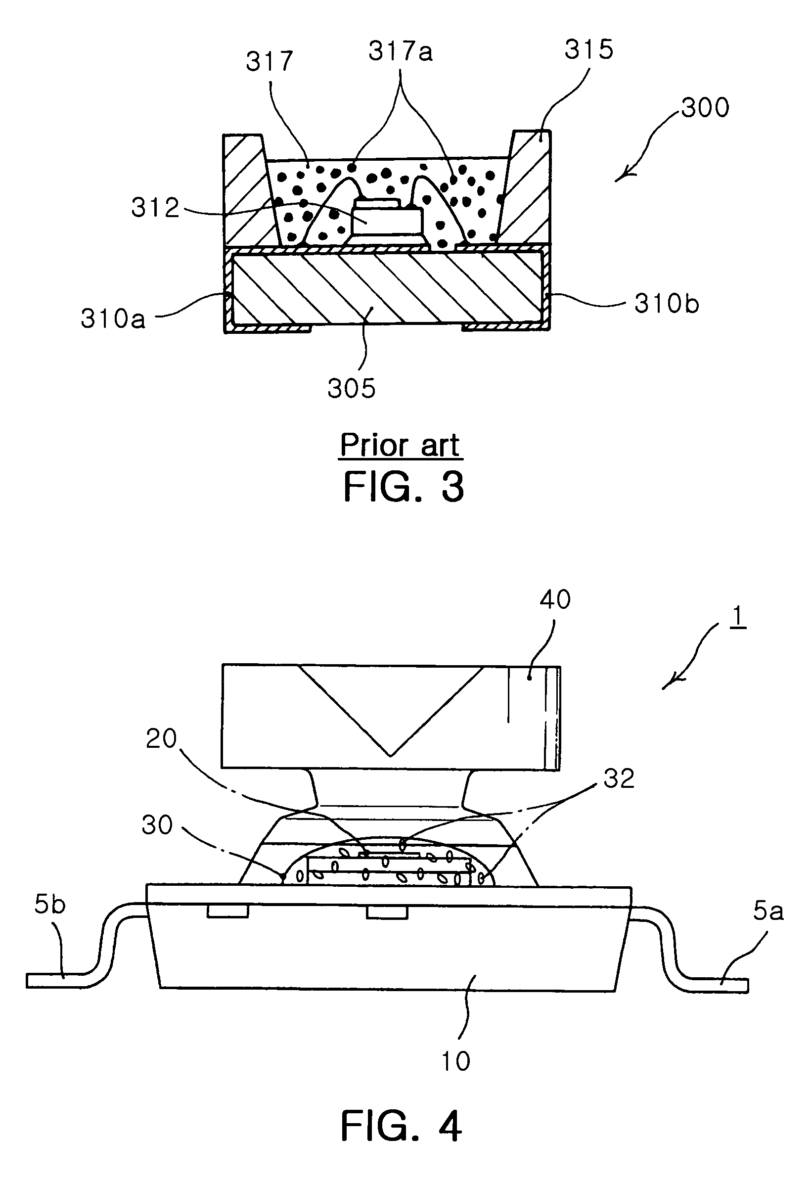
[0049]As shown in FIG. 4, an LED package 1 using a diffuser according to the present invention has a substrate 10 with electrodes 5a and 5b formed thereon. The substrate 10 preferably has a planar structure molded with molding material, and has each of the electrodes 5a and 5b formed thereon to provide power to an LED chip 20 described later.

[0050]The LED chip 20 is mounted on an upper part of the substrate 10 and electrically connected to the electrodes 5a and 5b by wire bonding, etc. The invention is applicable to either a horizontal type of LED chip 20 with all electric terminals formed on an upper surface thereof, or a vertical type of LED chip 20 with electric terminals formed on both upper and lower surfaces thereof.

[0051]In addition, a step 25 is formed on an upper surface of the substrate 10 to surround the portion where the LED-chip 20 is mounted....


PUM


Abstract

The invention relates to an LED package for facilitating color mixing using a diffuser and a manufacturing method of the same. The LED package includes a substrate with an electrode formed thereon, and an LED chip mounted on the substrate. The LED package also includes an encapsulant applied around the light emitting diode chip, containing a diffuser. The LED package further includes a lens part disposed on the light emitting diode chip and the encapsulant to radiate light in a wide angle. The LED package allows light from the light emitting diode chip to be emitted out of the package without distortion. The invention allows light to exit through the encapsulant containing the diffuser and the lens part, achieving uniform diffusion and emission of light from the LED chip, thereby increasing a radiating angle and obtaining a uniform light source.

Description

CLAIM OF PRIORITY[0001]This application claims the benefit of Korean Patent Application No. 2005-67859 filed on Jul. 26, 2005, in the Korean Intellectual Property Office, the disclosure of which is incorporated herein by reference.BACKGROUND OF THE INVENTION[0002]1. Field of the Invention[0003]The present invention relates to a Light Emitting Diode (LED) package incorporating a diffuser to facilitate color mixing and to a manufacturing method of the same. More particularly, the invention relates to an LED package in which a diffuser is applied to an encapsulant disposed in an upper part of an LED chip to achieve color mixing, enabling uniform emission without distortion of light from the LED chip in a wide radiating angle, thereby facilitating color mixing while reducing a thickness and enhancing a degree of freedom of a lens part, and to a manufacturing method of the same.[0004]2. Description of the Related Art[0005]In general, various sizes of LED packages are used for backlight u...

Claims


Application Information

Patent Timeline
Patent Type & Authority Patents(United States)
IPC IPC(8): H01L27/15H01L31/12H01L33/00H01L33/54H01L33/50H01L33/56H01L33/60H01L33/62
CPCH01L33/58H01L33/505H01L2933/0091H01L2924/181H01L2224/48091H01L2224/49107H01L2224/73265H01L2924/00014H01L2924/00012
Inventor HAN, SEONG YEONLEE, SEON GOOSONG, CHANG HOPARK, JUNG KYUPARK, YOUNG SAMHAN, KYUNG TAEG
Owner SAMSUNG ELECTRONICS CO LTD
Why Eureka
Try Eureka