

Compound for organic optoelectronic device, organic light emitting diode including the same, and display including the organic light emitting diode
a technology of organic materials, which is applied in the direction of solid-state devices, semiconductor devices, organic chemistry, etc., can solve the problems of inefficient the development of organic material layers forming materials for organic light emitting diodes has so far not been satisfactory, so as to improve the efficiency of the combination of holes and electrons, improve the life-span, and improve the efficiency.
- Summary
- Abstract
- Description
- Claims
- Application Information
AI Technical Summary
Benefits of technology
Problems solved by technology
Method used
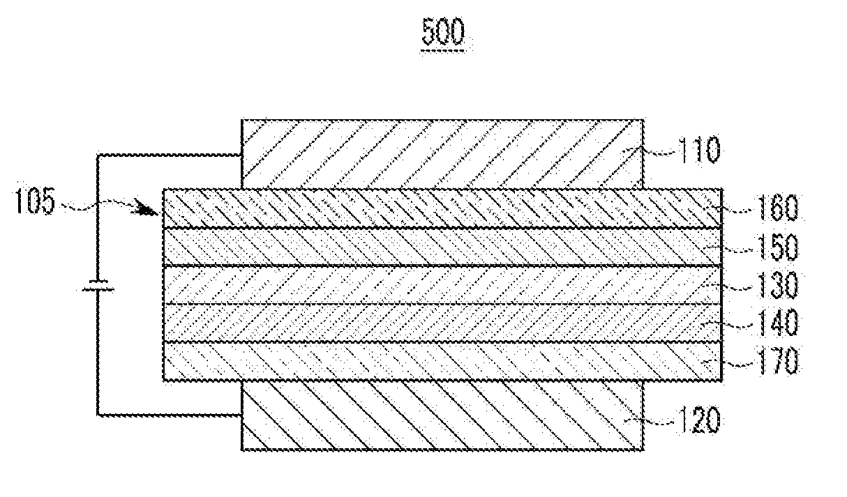
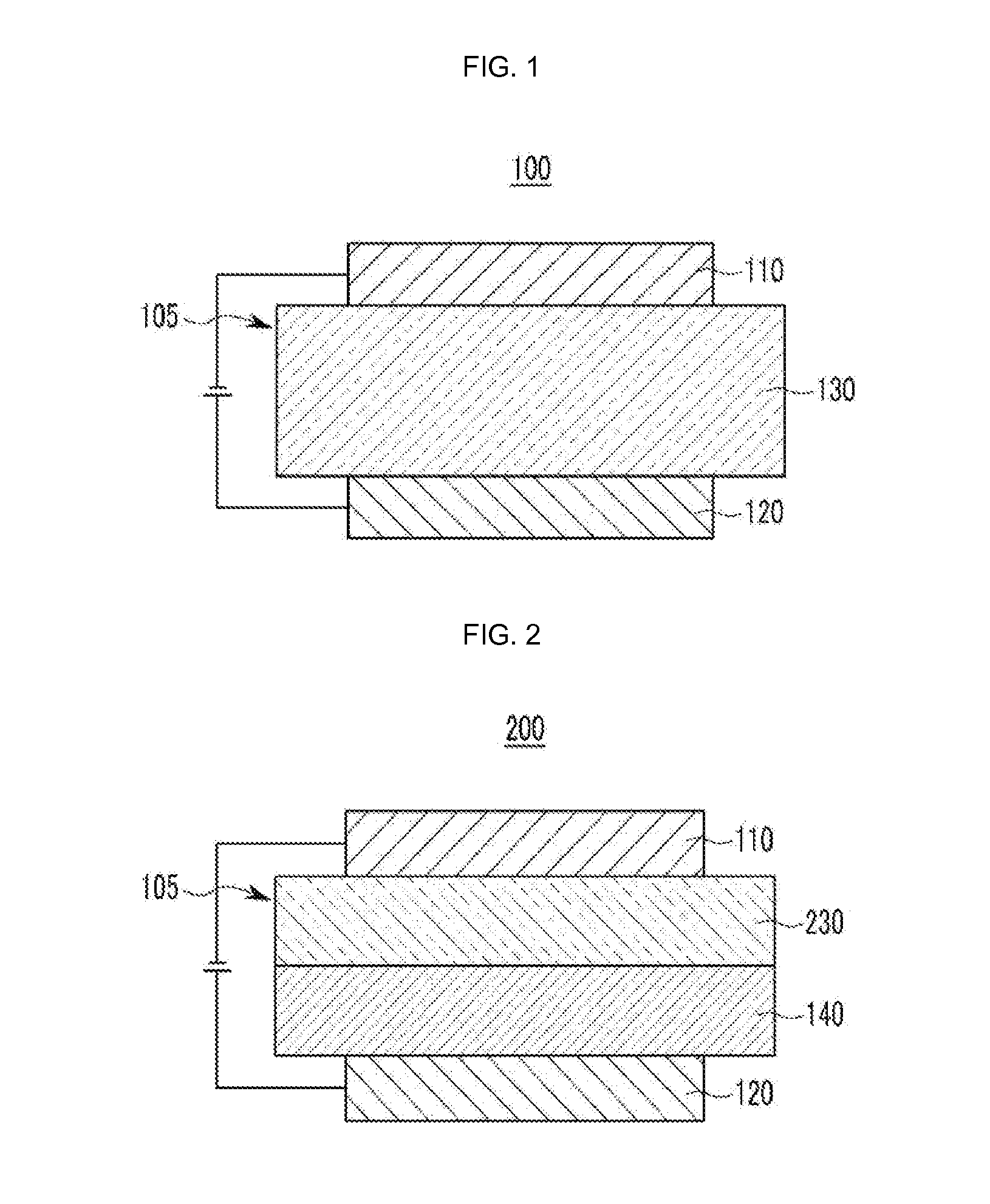
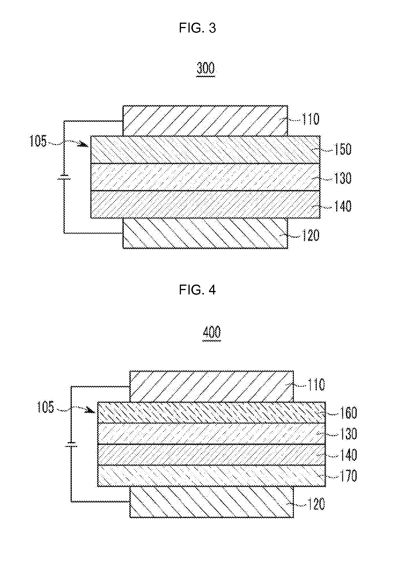
Image

Examples
example 1
Synthesis of Compound A-5
[0250]The compound A-5 as an example of a compound for an organic optoelectronic device according to the present disclosure is synthesized according to the following Reaction Scheme 1.
Synthesis of Chemical Formula A-5 Compound
[0251]20 g (50.090 mmol) of a compound A, 20.346 g (55.099 mmol) of a compound B, 5.788 g (5.009 mmol) of tetrakis(triphenylphosphine)palladium (0), and 19.8 g (143.258 mmol) of potassium carbonate are suspended in THF / toluene / distilled water mixed in a ratio of 150 / 150 / 150 mL, and then refluxed and agitated for 18 hours. When the reaction is complete, the obtained mixture is slowly poured into 2 L of methanol to produce a precipitate. The precipitate is filtered and washed with methanol and distilled water. Next, the precipitate is dried and then dissolved in dichloromethane (CH2Cl2) and separated through silica gel chromatography. Accordingly, 15.47 g of a compound A-5 is obtained (a yield of 55%).
[0252]1H-NMR (600 MHz, CDCl3): 8.97 (...
example 2
Synthesis of Compound A-18
[0253]
Synthesis of Chemical Formula A-18 Compound
[0254]The same reaction as aforementioned except for using 24.539 g (50.090 mmol) of a compound C instead on the compound B in Example 1 is performed. Then, 19.81 g of a compound A-18 (a yield of 62%) is obtained through recrystallization using dichloromethane instead of the silica gel chromatography.
example 3
Synthesis of Compound A-151
[0255]
Synthesis of Chemical Formula A-151 Compound
[0256]The same reaction as aforementioned in Example 1 is performed except for using 24.539 g (50.090 mmol) of a compound D instead of the compound B. Then, 16.61 g of a compound A-151 (a yield of 52%) is obtained through recrystallization using dichloromethane instead of silica gel chromatography.
PUM
| Property | Measurement | Unit |
|---|---|---|
| triplet excited energy | aaaaa | aaaaa |
| light emitting wavelength | aaaaa | aaaaa |
| thermal decomposition temperature | aaaaa | aaaaa |
Abstract
Description
Claims
Application Information