Electronic component device and manufacturing method therefor

Inactive Publication Date: 2005-08-23
MURATA MFG CO LTD
View PDF13 Cites 7 Cited by
  • Summary
  • Abstract
  • Description
  • Claims
  • Application Information

AI Technical Summary

Benefits of technology

[0015]Accordingly, in order to overcome the problems described above, preferred embodiments of the present invention provide an electronic component device that is capable of making displacements of wiring lines due to ultrasonic vibration substantially uniform and is also capable of bringing all wiring lines into substantially a uniform bonding state, even when wiring lines are arranged at a high density, and also provide a method for manufacturing the same.

Problems solved by technology

This causes a problem in that, when much time is spent applying ultrasonic waves until all wiring lines are sufficiently bonded, the wiring lines that are bonded earlier begin to crack.
While ultrasonic vibration is applied, displacements repeatedly occur, thereby causing a difference in bondability between the perpendicular wiring line and the parallel wiring line.
In this case, however, the connecting section of each of the perpendicular wiring lines must be formed wider and, therefore, if wiring lines are arranged at a high density, it is difficult to secure a sufficient formation width.
This make it difficult to bring all wiring lines into a uniform bonding state.

Method used


Image

  • Electronic component device and manufacturing method therefor
  • Electronic component device and manufacturing method therefor
  • Electronic component device and manufacturing method therefor

Examples


Embodiment Construction

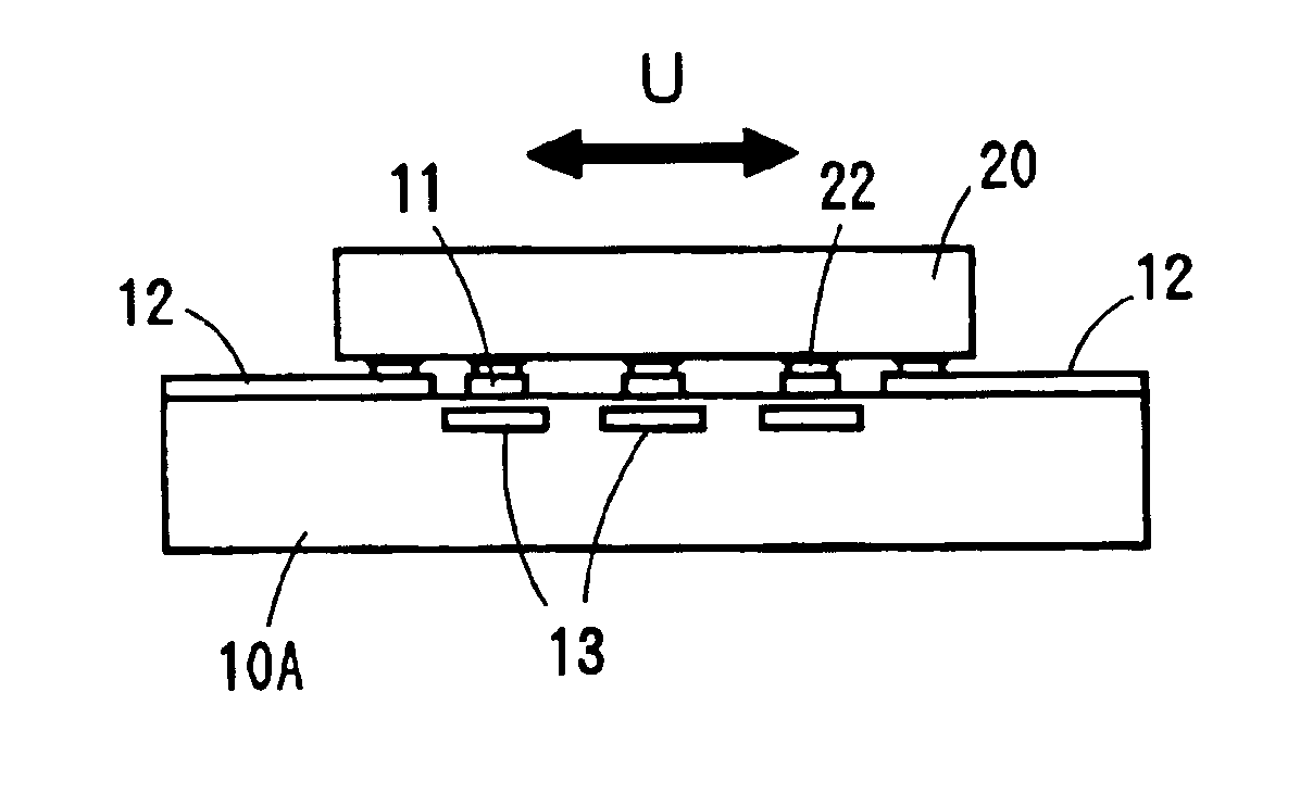
[0042]An electronic component device according to a first preferred embodiment of the present invention will be described with reference to FIGS. 6 to 8. FIG. 6 is a plan view of this electronic component device. FIG. 7 is a side view of the electronic component device. FIGS. 8A and 8B are each an enlarged sectional view of a bonding portion.

[0043]A board 10A preferably includes an organic board made of a material such as glass epoxy resin or bismaleimide triazine (BT) resin, a ceramic board such as alumina, or a crystal board made of silicon or other suitable material. A plurality of wiring lines 11 and 12 that extend along directions that substantially perpendicularly intersect each other is formed on the board 10A. As shown in FIG. 6, each of the wiring lines 11 is arranged so as to form an angle θ1 with respect to a direction of ultrasonic vibration U (described below) that is larger than approximately 45° (θ1>45°), and each of the wiring lines 12 is arranged to form an angle θ2...


PUM


Abstract

In an electronic component device, electrodes of an electric component and respective wiring lines on a board are collectively bonded together via bumps using ultrasonic vibration. The wiring lines include wiring lines that are substantially parallel to the direction of ultrasonic vibration and wiring lines that are substantially perpendicularly to the direction of ultrasonic vibration. A displacement inhibiting layer is provided inside the board in a portion below the wiring lines that are substantially perpendicular to the direction of ultrasonic vibration.

Description

BACKGROUND OF THE INVENTION[0001]1. Field of the Invention[0002]The present invention relates to an electronic component device formed by mounting an electronic component on a board via bumps, and more specifically, the present invention relates to an electronic component device implemented by using a flip chip bonding method.[0003]2. Description of the Related Art[0004]To date, regarding a flip chip bonding method for bonding bumps and respective wiring patterns on a board together, Japanese Unexamined Patent Application Publication No. 63-288031 discloses a flip chip bonding method in which bumps formed on respective electrodes of a semiconductor chip are aligned with respective wiring patterns on a board disposed on a heated stage, and in which pressure and ultrasonic vibration are applied to the rear surface of the chip via a tool, thereby bonding the bumps and the respective wiring patterns together.[0005]FIG. 1 shows an example of an electronic component device. FIG. 2 illustr...

Claims


Application Information

Patent Timeline
IPC IPC(8): H01L21/02H01L21/60H05K1/02H05K3/32
CPCH01L24/81H05K1/0271H01L2224/16225H01L2224/81205H01L2224/81801H01L2924/01013H01L2924/01029H01L2924/01033H01L2924/01079H01L2924/19041H01L2924/19043H01L2924/3025H05K3/328H05K2201/10416H05K2201/10674H05K2201/2009H05K2201/2045H05K2203/0285H01L2924/01005H01L2924/01006H01L2924/01047H01L2924/014H01L2924/15787H01L2224/81206H01L2924/14H01L2224/05573H01L2224/05568H01L2924/00H01L2224/05624H01L2924/00014F04B39/1066F04B39/0027
Inventor MAEDA, TAKENOBU
Owner MURATA MFG CO LTD
Why Eureka
Try Eureka