Self-luminous device and electric machine using the same

a self-luminous device and electric machine technology, applied in the direction of static indicating devices, discharge tubes luminescnet screens, instruments, etc., can solve the problems of inability to play the intended role of el elements intended for the same scale in gray scale display, helpless against fluctuation in characteristic of tfts, and the disadvantage of analog gray scale methods

Inactive Publication Date: 2005-08-30
SEMICON ENERGY LAB CO LTD
View PDF26 Cites 175 Cited by
  • Summary
  • Abstract
  • Description
  • Claims
  • Application Information

AI Technical Summary

Benefits of technology

[0019]According to the present inventors' opinion, in order to obtain a pixel structure unsusceptible of fluctuation in TFT characteristic, a digital-driven gray scale method in which a current controlling TFT is used merely as a switching element for controlling current is more advantageous than the conventional analog-driven gray scale method in which how much light is emitted from an EL element is controlled by controlling the amount of current.
[0052]As described above, a feature of the present invention is that, by using the digital-driven time division gray scale method in an active matrix self-luminous device, an image can be displayed in gray scale without being affected by TFT characteristics, which has been the problem in analog-driven gray scale display. Moreover, the present invention is successful in improving the aperture ratio of the pixels by arranging in a specific manner the storage capacitor formed in each pixel in the pixel portion in order to diminish fluctuation in characteristic of TFTs.

Problems solved by technology

However, the analog gray scale method has a drawback and it is helpless against fluctuation in characteristic of TFTs.
Therefore different amounts of current flow in the two EL elements thereof to cause them to emit different amounts of light, with the result that the EL elements intended for the same scale in gray scale display now cannot play their intended roles.
Therefore if there is even a slightest difference in Id-Vg characteristic, equality in gate voltage does not always assure equality in amount of current outputted.
The analog gray scale method is thus extremely sensitive to the fluctuation in characteristic of the TFTs, which forms an obstacle toward achieving multi-color display in conventional active matrix self-luminous devices.

Method used


Image

  • Self-luminous device and electric machine using the same
  • Self-luminous device and electric machine using the same
  • Self-luminous device and electric machine using the same

Examples


embodiment 1

[Embodiment 1]

[0142]Embodiments of the present invention will be described with reference to FIGS. 9 to 16 and Tables 1 to 4. Descriptions here are about: a pixel portion used in carrying out the present invention; the structure and specifications (size, voltage values, etc.) of driver circuits provided in the periphery of the pixel portion; and signals to be inputted thereto.

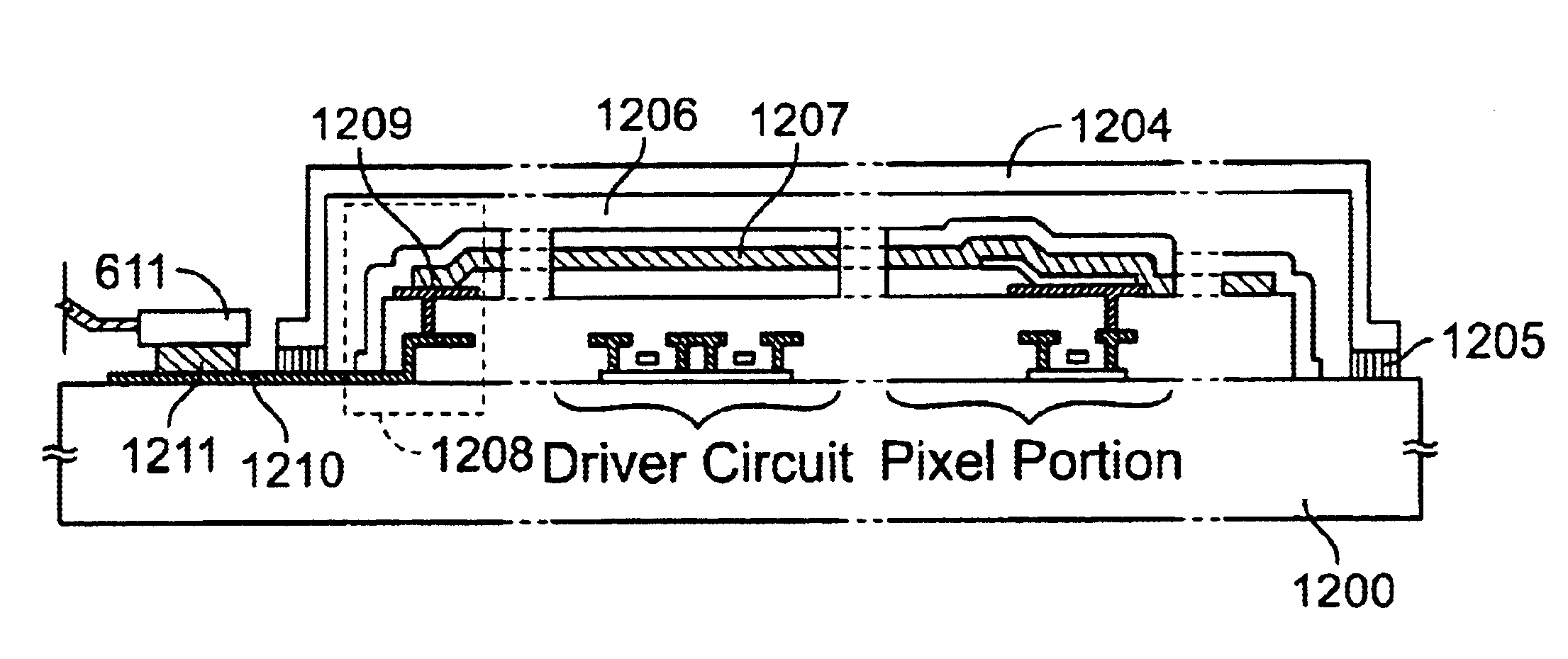
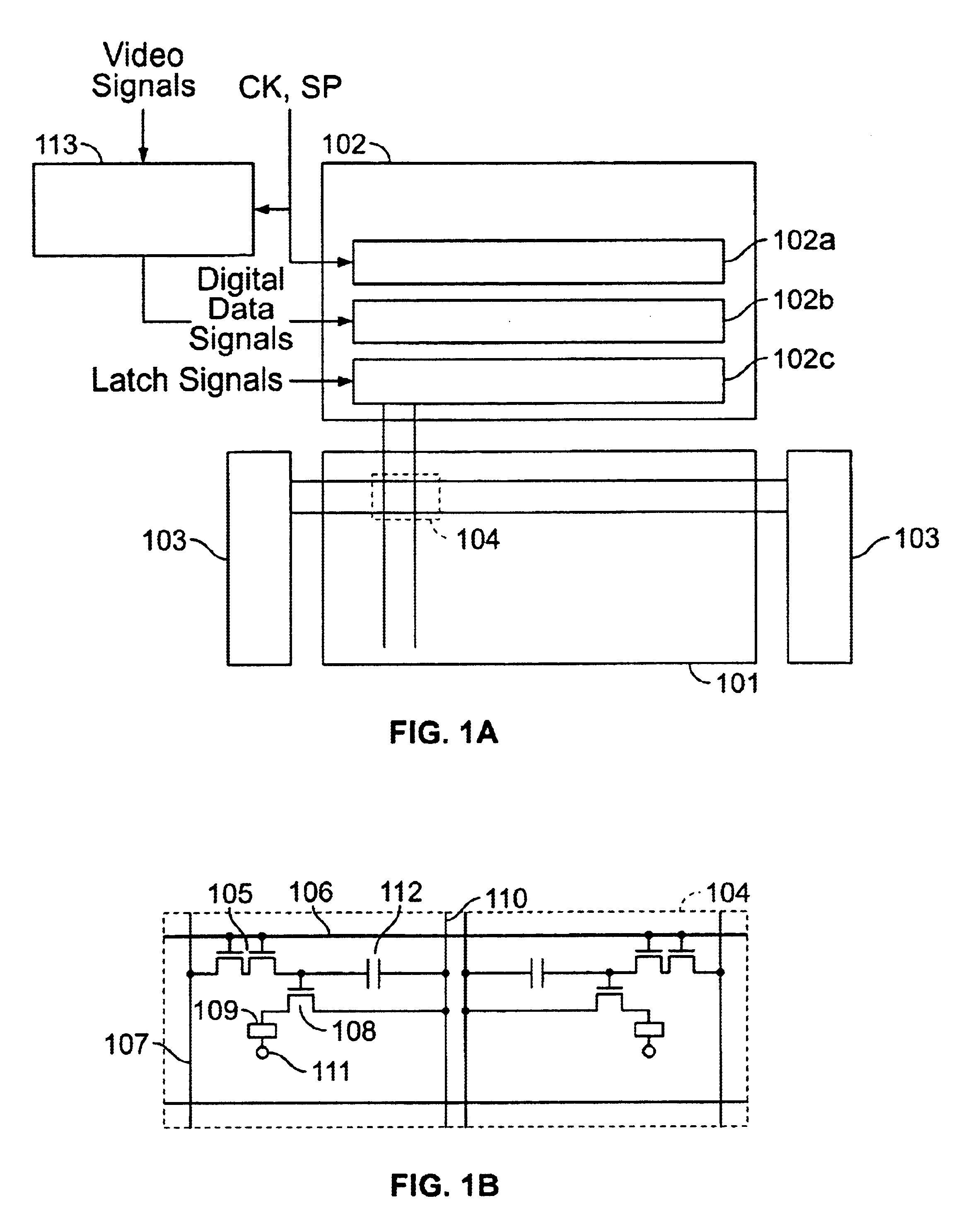
[0143]FIG. 9 is a plan view of the entire panel showing its top (the side of the panel on which a cathode is to be formed). Accordingly, the side for display is the bottom in FIG. 9. Reference symbol 901 in FIG. 9 denotes a pixel portion, 902, a source driver circuit, 903, gate driver circuits, and 904, flexible printed circuit (hereinafter abbreviated as FPC) input portions. The FPC used in this embodiment is 500 μm in pitch and has 50×2 terminals.

[0144]In this embodiment, a protective circuit for an FPC input portion as the one shown in FIG. 10 is provided in some of FPC input portions (1) 904a and FPC input ...

embodiment 2

[Embodiment 2]

[0164]In Embodiment 1, the power source (709 in FIG. 7) for applying voltage to the EL element provided outside the panel is turned off during the display periods whereas the power source is turned on during the writing periods. According to this method, the power source is turned on upon the start of the display period after the writing period, resulting in rapid increase in current flow. It sometimes surpasses the ability of a variable voltage source for charging the load of the entire panel.

[0165]As a result, the necessary voltage cannot be applied to the entire panel to make the display quality of the panel unsatisfiable.

[0166]In order to prevent the rapid increase in current between the writing period and the display period, the power supply (709 in FIG. 7) is kept on in Embodiment 2.

[0167]However, this method leads to all-time display including the writing periods. If the display periods are shorter than the writing periods such as Writing 4, Writing 5, and Writi...

embodiment 3

[Embodiment 3]

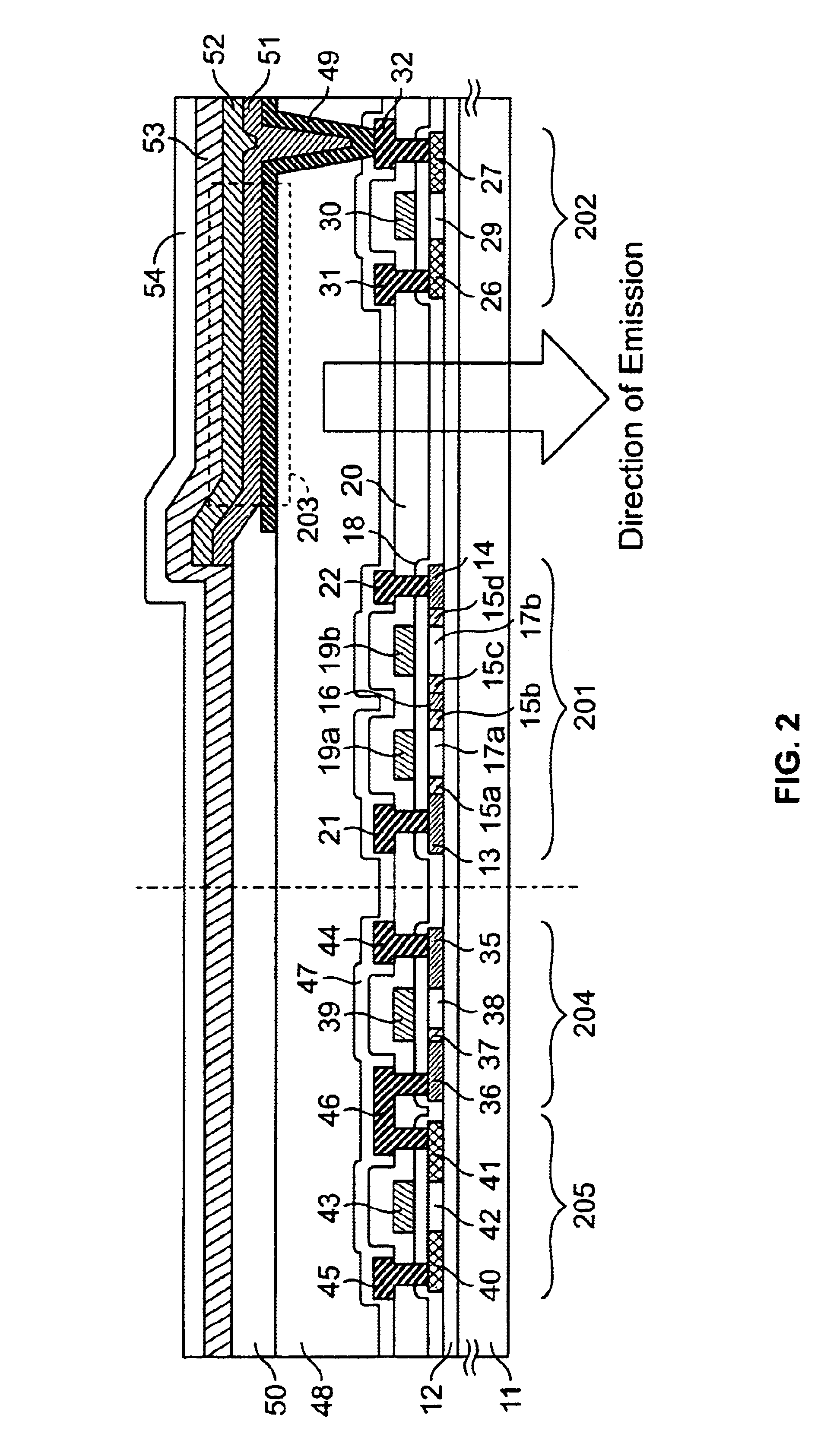
[0169]Embodiment 3 of the present invention will be described with reference to FIGS. 13A to 15C. Given here is a description on a method of manufacturing simultaneously TFTs of a pixel portion and TFTs of driver circuits provided in the periphery of the pixel portion. To simplify the description, a CMOS circuit that is a base unit is shown as the driver circuits.

[0170]First, as shown in FIG. 13A, a base film 501 is formed to a thickness of 300 nm on a glass substrate 500. In this embodiment, layered silicon oxynitride films are used as the base film 501. At this point, the layer of the base film which comes into contact with the glass substrate 500 contains a 10 to 25 wt % of nitrogen. It is effective to give the base film 501 a heat releasing effect, and a DLC (diamond-like carbon) film may be provided.

[0171]Next, an amorphous silicon film with a thickness of 50 nm (not shown) is formed on the base film 501 by a known film deposition method. There is no need to limit...


PUM


Abstract

To provide a self-luminous device capable of clear, multi-gray scale, color display and an electric machine provided with the same. Gray scale display is attained by a time division driving method in which an EL element (109) provided in a pixel (104) is controlled to emit light or not to emit light by means of time, thereby avoiding being affected by fluctuation in characteristic in current controlling TFTs (108).

Description

BACKGROUND OF THE INVENTION[0001]1. Field of the Invention[0002]The present invention relates to a self-luminous device (or an EL display device) manufactured by forming a light emitting element (such as an EL (Electro Luminescence) element) on a substrate, and an electric machine having the self-luminous device as a display (display unit). The light emitting element here is also called an OLED (Organic Light Emitting Device).[0003]The light emitting element has a layer containing an EL material that can provide EL (Electro Luminescence: the luminescence generated by applying an electric field) (hereinafter referred to as EL layer), in addition to an anode and a cathode. The luminescence generated from an EL material includes light emission (fluorescence) upon returning from the singlet excitation to the ground state and light emission (phosphorescence) upon returning from the triplet excitation to the ground state. The self-luminous device of the present invention can use both type...

Claims


Application Information

Patent Timeline
Patent Type & Authority Patents(United States)
IPC IPC(8): G09G3/20G09G3/30G09G3/32H01L27/32
CPCG09G3/2018G09G3/2022G09G3/30G09G3/3233G09G3/3258G09G3/3266G09G3/3291G09G2300/0426G09G2300/0465G09G2300/0842G09G2300/0861G09G2300/0866G09G2320/0233G09G2320/029G09G2320/043H10K59/1216H10K59/1213H10K59/12
Inventor KOYAMA, JUNINUKAI, KAZUTAKA
Owner SEMICON ENERGY LAB CO LTD
Why Eureka
Try Eureka