Light emitting diode package

a technology of light-emitting diodes and diodes, which is applied in the direction of refractors, semiconductor/solid-state device details, lighting and heating apparatus, etc., can solve the problems of increasing processing complexity and reducing production costs, and achieves improved front surface illumination. the effect of improving the amount of illumination and facilitating manufacturing

Active Publication Date: 2005-08-30
LEXTAR ELECTRONICS CORP
View PDF3 Cites 65 Cited by
  • Summary
  • Abstract
  • Description
  • Claims
  • Application Information

AI Technical Summary

Problems solved by technology

In addition, the manufacturing convenience is kept when performing packaging process so that processing complexity is not increased.

Method used


Image

  • Light emitting diode package
  • Light emitting diode package
  • Light emitting diode package

Examples


Embodiment Construction

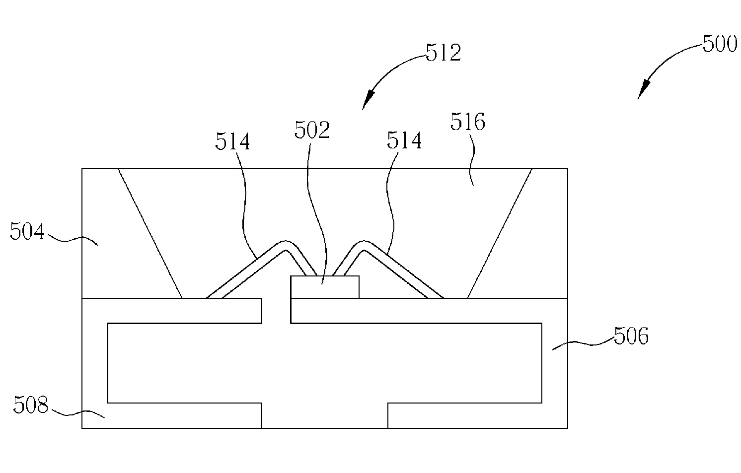
[0026]Please refer to FIG. 3. FIG. 3 is a schematic diagram of a scatterer supported wavelength converter 100 according to a first preferred embodiment of the present invention. As shown in FIG. 3, the present invention scatterer supported wavelength converter 100 is a physical composite material or a chemical composite material. The scatterer supported wavelength converter 100 comprises a scatterer 102 and a plurality of wavelength converting activators 104 having a physical or chemical bonding therebetween. Each of the wavelength converting activators 104 adheres to portions of a surface of the scatterer 102. The wavelength converting activator 104 is a wavelength converting material, and the scatterer 102 is a scattering material for repetitively scattering and diffusing light beams. In addition, different phases may exist in the interface between the phase of the scatterer 102 and the phase of the wavelength converting activator 104.

[0027]Please refer to FIG. 4. FIG. 4 is a sche...


PUM


Abstract

A light emitting diode package includes a light emitting diode device disposed in the light emitting diode package, and a molding material covering the light emitting diode device. The molding material includes a plurality of scatter supported wavelength converters. Portions of light beams emitted from the light emitting diode device incident to each of the scatter supported wavelength converters are scattered by each of the scatter supported wavelength converters and absorbed to excite each of the scatter supported wavelength converters to emit light in another wavelength.

Description

BACKGROUND OF INVENTION[0001]1. Field of the Invention[0002]The invention relates to a light emitting diode package, and more particularly, to a light emitting diode package having scatterer supported wavelength converters embedded in a molding material and having superior illumination uniformity and manufacturing convenience.[0003]2. Description of the Prior Art[0004]Recently, the new application fields of high illumination light emitting diodes (LEDs) have been developed. Different from a common incandescent light, a cold illumination LED has the advantages of low power consumption, long device lifetime, no idling time, and quick response speed. In addition, since the LED also has the advantages of small size, vibration resistance, being suitable for mass production, and being easily fabricated as a tiny device or an array device, it has been widely applied in display apparatuses and indicating lamps of information, communication, and consumer electronic products. The LEDs are not...

Claims


Application Information

Patent Timeline
Patent Type & Authority Patents(United States)
IPC IPC(8): H01L33/00F21V5/00F21V9/40H01L23/28H01L25/16H01L33/50H01L33/52H01L33/60H01L33/62
CPCH01L33/502H01L25/167H01L33/501H01L2933/0091H01L2224/48247H01L2924/12032H01L2224/48091H01L2924/00014H01L2924/00H01L2224/8592H01L2924/181H01L2224/48257H01L2924/00012
Inventor CHANG, CHIH-CHINHSIEH, HSIANG-CHENGHUANG, TENG-HUEI
Owner LEXTAR ELECTRONICS CORP
Why Eureka
Try Eureka