Bare die carrier

a carrier and die technology, applied in the field of die carriers, can solve the problems of reducing manufacturing costs, rework, and identification of defective integrated circuit chips, and achieve the effect of easy reaching

Inactive Publication Date: 2005-08-30
SV PROBE PTE LTD
View PDF43 Cites 12 Cited by
  • Summary
  • Abstract
  • Description
  • Claims
  • Application Information

AI Technical Summary

Benefits of technology

[0014]The new carrier provides I/O pads which can be easily reached by circuit probes. There is no need to use expensive intermediate circuitry such as a PGA to communicate test signals with the carrier. The carrier can be easily dropped in a standard burn-in test socket so that the die in the carrier can be tested and burned in. The alignment fence obviates the need to visually align the die with the interconnect circuit. The n...

Problems solved by technology

A major challenge in the production of multichip modules is the identification of defective integrated circuit chips.
The testing of die prior to packaging or assembly into multichip modules reduces the amount of rework which in turn decreases manufacturing costs.
Such defects can cause early failure.
One problem with the testing of bare die is that as circuit dimensions have become smaller, so have the pads on the die surfaces.
As a result, it sometimes can be impractical to use devices such as probe cards to make electrical contact with die pads for testing purposes.
Another problem with probe cards has been their relatively poor performance in testing high frequency signals.
The use of gold, however, can be too expensive for many semiconductor processes.
Although the die can be removed from the package after testing by removal of the wire bonds, this can result in d...

Method used


Image

  • Bare die carrier
  • Bare die carrier
  • Bare die carrier

Examples


Embodiment Construction

[0030]The present invention comprises a novel carrier for use in testing bare semiconductor circuit die. The following description is presented to enable any person skilled in the art to make and use the invention, and is provided in the context of a particular application and its requirements. Various modifications to the preferred embodiment will be readily apparent to those skilled in the art, and the generic principles defined herein may be applied to other embodiments and applications without departing from the spirit and scope of the invention. Thus, the present invention is not intended to be limited to the embodiment shown, but is to be accorded the widest scope consistent with the principles and features disclosed herein.

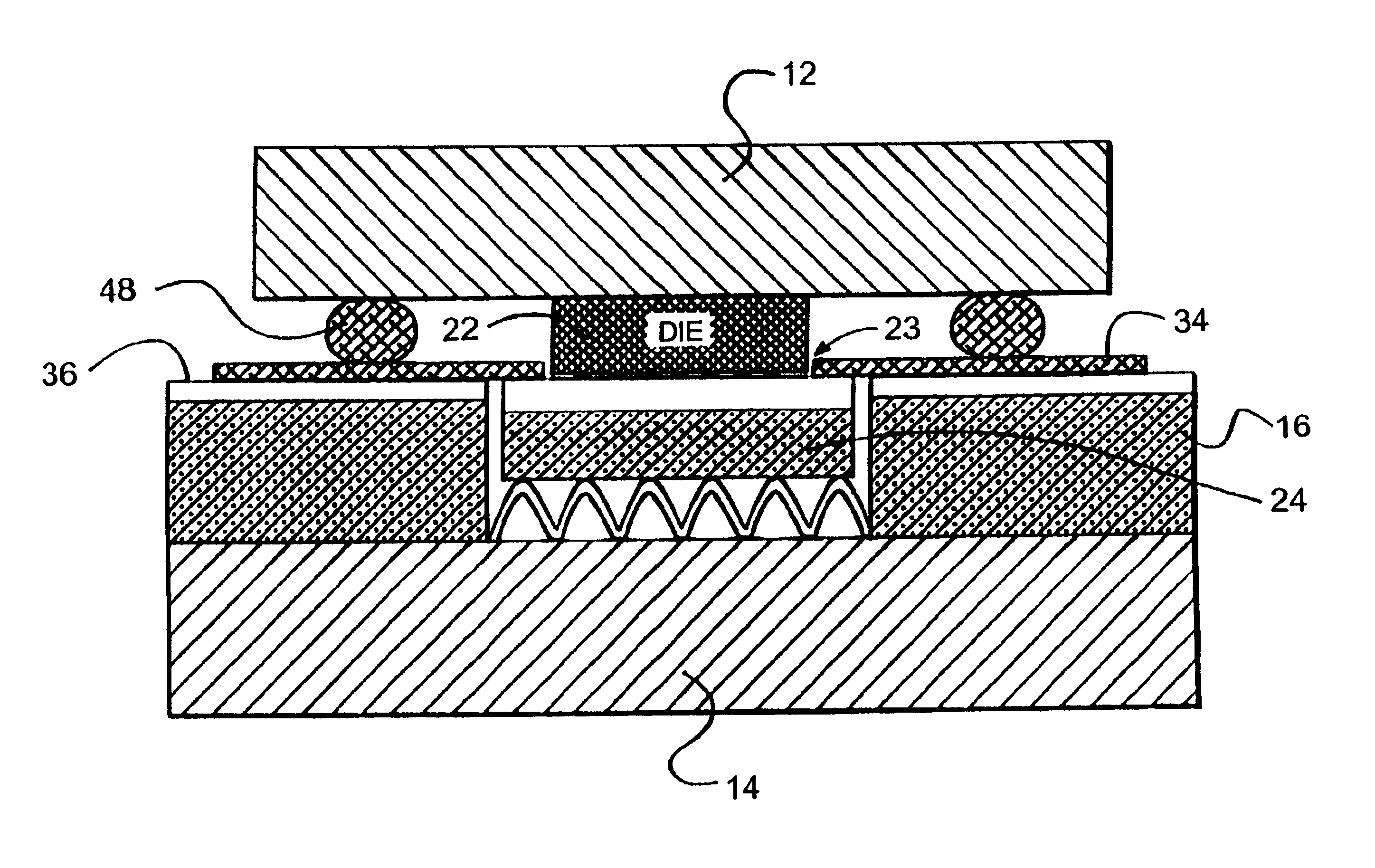
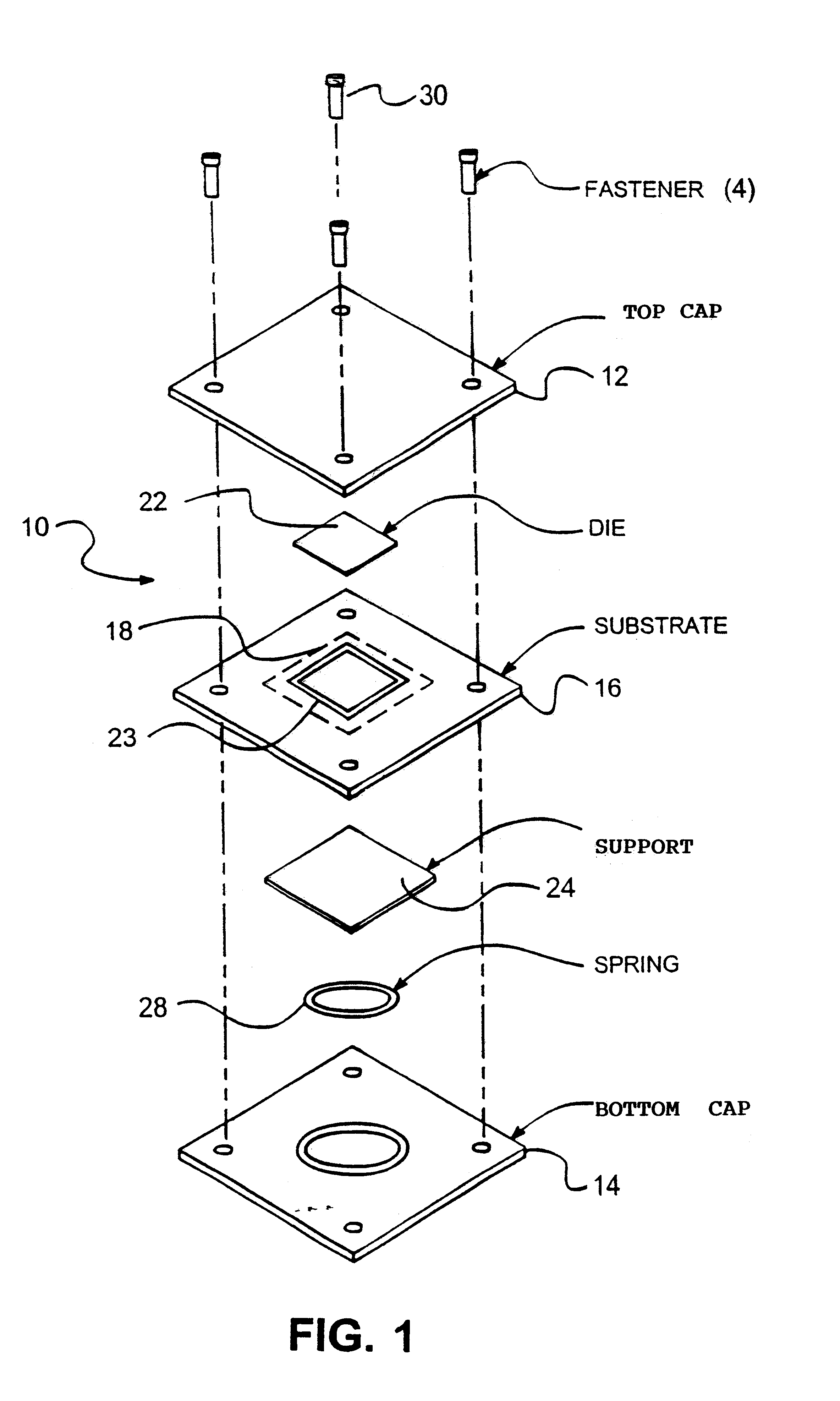
[0031]Referring to the illustrative drawings of FIG. 1, there is shown an exploded perspective view of a bare semiconductor circuit die carrier 10 in accordance with the present invention. The carrier 10 includes a top cap 12, a bottom cap 14 and a substrat...


PUM


Abstract

A bare semiconductor circuit die carrier is provided for use in the test of semiconductor circuits, the carrier, comprising: a substrate defining an opening and an outer perimeter; a multiplicity of I/O pads disposed about the perimeter; an interconnect circuit which includes a composite of a multiplicity of individual electrical conductors which are formed in a polymer dielectric; wherein the interconnect circuit overlays a top surface of the substrate and extends across the opening so as to form a flexible membrane that spans the opening; a multiplicity of die contact pads connected to the conductors are disposed about the flexible membrane with particles deposited on the die contact pads; a fence upstanding from the membrane and sized to receive a test die; a top cap that rests upon the die when the die is received within the fence; a bottom cap that rests against a bottom surface of the substrate; and a fastener for securing the top cap to the bottom cap with the die disposed therebetween.

Description

[0001]This application is a continuation of application Ser. No. 08 / 542,685, filed Oct. 13, 1995, now U.S. Pat. No. 6,049,215 which is a continuation of application Ser. No. 08 / 408,048, filed Mar. 21, 1995, now abandoned, which is a continuation of Ser. No. 07 / 979,719, filed Nov. 20, 1992, now U.S. Pat. No. 5,402,077.BACKGROUND OF THE INVENTION[0002]1. Field of the Invention[0003]The invention relates generally to the testing of semiconductor circuits and more particularly, to die carriers used to make electrical contact with the pads of a bare semiconductor circuit die during functional and burn-in testing.[0004]2. Description of the Related Art[0005]A major challenge in the production of multichip modules is the identification of defective integrated circuit chips. The yield rate of multichip modules can be significantly increased through the use of fully tested and burned-in die. The testing of die prior to packaging or assembly into multichip modules reduces the amount of rework...

Claims


Application Information

Patent Timeline
IPC IPC(8): G01R1/04G01R1/02G01R31/28
CPCG01R1/0483G01R31/2884
Inventor AGAHDEL, FARIBORZGRISWOLD, BRADHUSAIN, SYEDMOTI, ROBERTROBINETTE, JR., WILLIAM C.HO, CHUNG W.
Owner SV PROBE PTE LTD
Why Eureka
Try Eureka