Logic circuit having a functionally redundant transistor network

Inactive Publication Date: 2005-08-30
OPEN-SILICON
View PDF6 Cites 8 Cited by
  • Summary
  • Abstract
  • Description
  • Claims
  • Application Information

AI Technical Summary

Benefits of technology

[0027]Thus, the present invention pertain to a new family of transistor-based logic circuits based on methods of interconnecting transistors, and more generally, switches. The method of the present invention employs the selecti

Problems solved by technology

Pseudo-NMOS is not fast, it dissipates static power in a steady state (i.e., when the output is in the low state), and is sensitive to noise.
Moreover, domino logic has a limited area occupancy due to low number of PMOS transistors therein.
However, it is not possible to implement inverting-structures and, as with all other dynamic logics, domino logic is subject to charge-sharing problems.
This type of logic has a lower area occupancy since there is no need for a static inverter, however it also has a lower operating speed due to the presence of PMOS transistors.
Since the output stage of every cell is also dynamic (i.e., a CMOS inverter), the NORA logic is more susceptible to charge-sharing problems than conventional domino logic
Hence, PTL suffers from losses in signal strength and is typically not applied in environments where noise margins are critical.
A key problem with conventional logic families is that their properties critically depend on the topology of the underlying transistor network implementations defining the logic family.
Note, this condition is not always guaranteed across all possible semiconductor fabrication processes and, other influencing sub-networks may be present.
However, if it is a design objective that both the A-Z and B-Z transitions be fast using the same IC logic topology, then conventional logic families do not offer a clear solution.
Therefore, such proposed methods are clearly applicable only for simple gates, and there exists no systematic method or system for constructing or identifying such structures having balanced rise and fall times using simplified gates and / or more complex gates.

Method used


Image

  • Logic circuit having a functionally redundant transistor network
  • Logic circuit having a functionally redundant transistor network
  • Logic circuit having a functionally redundant transistor network

Examples


Embodiment Construction

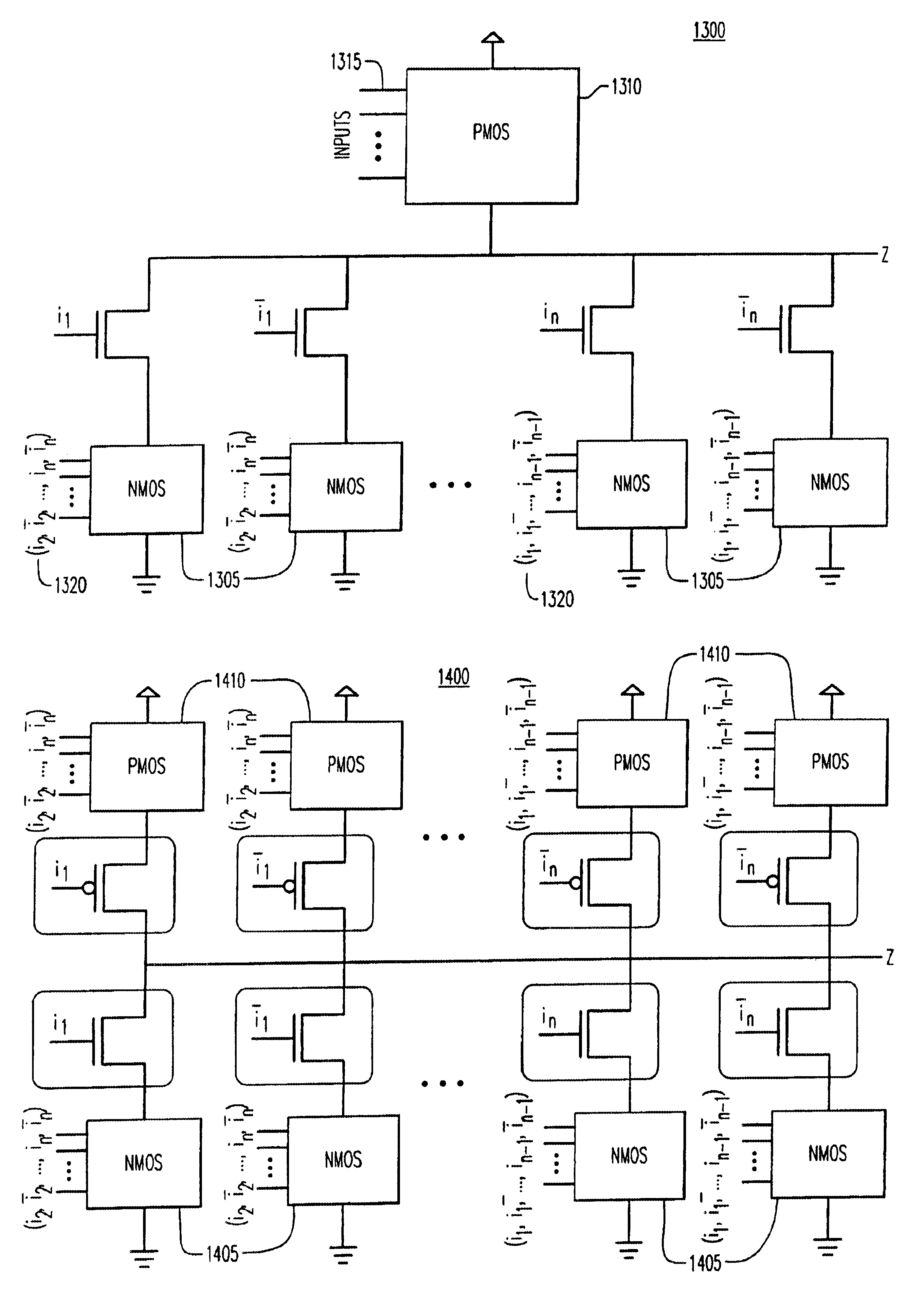
[0050]The present invention pertains to a new logic family for digital logic circuits based on the selective use of functionally redundant transistor configurations. Various configurations of functionally redundant transistor networks and a method based on functional decomposition for identifying and implementing functionally redundant transistor networks is presented herein.

[0051]In accordance with the present invention, a dynamic topology of transistors is formed from logic circuits having functionally redundant logic circuits to achieve specific target objectives.

[0052]Functionality for both simple gates and complex gates can be implemented by the logic family of the present invention. “Simple” gates implement the basic Boolean functionality of AND, OR, AND, NOR, NOT. “Complex” gates implement complex Boolean functionality, including interconnections of a multitude of simple Boolean gates. The implementation of complex gates may require a combination of one or more series and par...


PUM


Abstract

A method and system for constructing, designing, and using a family of logic circuits based on methods of interconnecting transistors (or more generally, switches). The method includes the selective use of functionally redundant transistors to achieve target objectives, such as speed of operation, power dissipation, control over switching capacitances, noise characteristics and signal integrity. In accordance with the present invention, multiple topologies may be incorporated into the implementation of a single dynamic transistor topology. The logic circuit family provides flexibility by implementing different topologies for the various functionally redundant sub-networks of transistors. The method is applicable to any network of transistors whose characteristics depend, at least in part, on its implementation topology.

Description

[0001]This application claims priority of U.S. Provisional Patent Application Ser. No. 60 / 269,006 filed on Feb. 15, 2001,BACKGROUND OF THE INVENTION[0002]1. Field of the Invention[0003]The present invention pertains to digital logic circuits and, in particular, to a method and system for designing digital logic circuits containing functionally redundant transistor networks used to design ICs (integrated circuits).[0004]2. Description of the Related Art[0005]Integrated circuit technology represents the core of electronic engineering technology. Transistors form the basic components from which ICs are fabricated. Several basic techniques for placing and interconnecting transistors are known. The most popular and effective technologies are based on MOS (metal oxide semiconductor) technology. Several logic families have been developed for digital logic design based on underlying MOS fabrication technology, such as, for example, CMOS (complementary metal oxide semiconductor), NMOS, and P...

Claims


Application Information

Patent Timeline
IPC IPC(8): G06F17/50
CPCG06F17/505G06F30/327
Inventor BOPPANA, VAMSIBHATTACHARYA, DEBASHIS
Owner OPEN-SILICON
Why Eureka
Try Eureka