Magnetic memory device

a memory device and magnetic technology, applied in semiconductor devices, digital storage, instruments, etc., can solve the problems of complicated measurement of sense current, difficult to select only a particular mram cell for read-out operation,

Active Publication Date: 2005-09-06
SAMSUNG ELECTRONICS CO LTD
View PDF7 Cites 68 Cited by
  • Summary
  • Abstract
  • Description
  • Claims
  • Application Information

AI Technical Summary

Benefits of technology

[0008]Briefly, a magnetic memory device embodiment of the present invention includes a magnetic memory cell that is switchable between two states of differing electrical resistance which are detectible by a sense current through the magnetic memory cell. The device includes a field effect transistor (FET) arrangement which has a source and a drain. The source and the drain are connected by a connecting element whic

Problems solved by technology

It is therefore difficult to select only a particular MRAM cell for a read-out operation.
Therefore, the sense currents are difficult to mea

Method used


Image

  • Magnetic memory device
  • Magnetic memory device
  • Magnetic memory device

Examples


Embodiment Construction

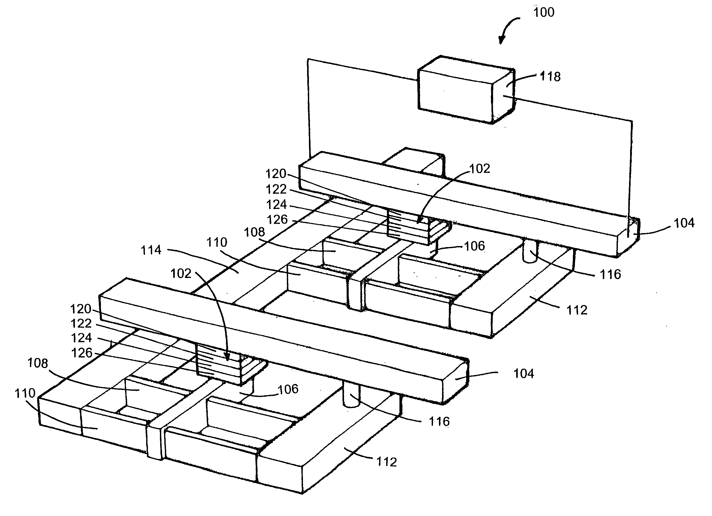
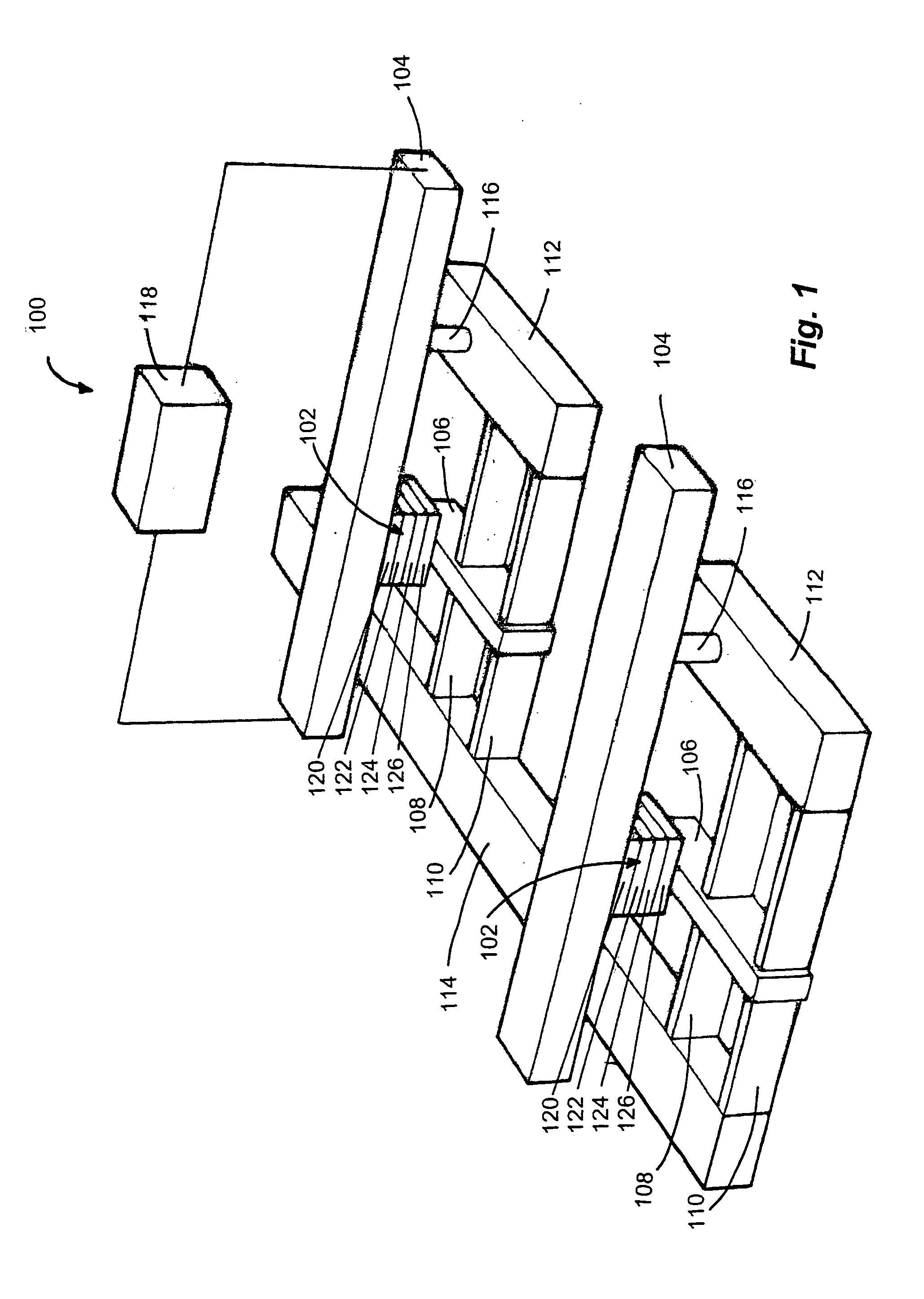
[0015]Referring initially to FIG. 1, a magnetic memory device (MRAM) 100 according to an embodiment is now described.

[0016]The MRAM 100 includes individual tunnelling magneto-resistance memory (TMR) cells 102. Each cell 102 is electrically connected with bit line 104. Each magnetic memory cell 102 is positioned on a gate electrode 106 which is in electrical contact with two connecting elements which in this embodiment are fins 108 and 110 of a finFET arrangement. The fins 108 and 110 connect source 114 and drain 112 of the finFET arrangement. In this embodiment the bit line 104 is electrically connected with drain 112 by connector 116.

[0017]When a current is applied along bit line 104, a magnetic field surrounds the bit line 104 which can be utilised to switch the magnetisation of the magnetic memory cell 102. FIG. 1 schematically indicates a circuit unit 118 that generates a voltage potential between the ends of bit line 104. In this embodiment the source 114 is operable as a word ...


PUM


Abstract

The present invention provides a magnetic memory device. An embodiment of the present invention includes a magnetic memory cell that is switchable between two states offering electrical resistance which are detectible by a sense current though the magnetic memory cell. The device includes a field effect transistor (FET) arrangement which has a source and a drain. The source and the drain are connected by a connecting element which projects from a portion of the device and which has an electrical conductivity that varies in response to a gate voltage applied to the connecting element. The magnetic memory cell is in electrical communication with the connecting element so that at least a portion of the sense current is in use associated with a corresponding gate voltage and the FET arrangement amplifies at least a portion of the sense current.

Description

FIELD OF THE INVENTION[0001]The present invention relates to a magnetic memory device and particularly, although not exclusively, to an array of magnetic memory cells.BACKGROUND OF THE INVENTION[0002]Non volatile magnetic random access memory (MRAM) devices have the potential to replace volatile dynamic random access memory (DRAM) devices and static random access memory (SRAM) devices in some applications. The MRAM devices typically comprise an array of memory cells such as tunnelling magneto-resistance (TMR), colossal magneto resistance (CMR), and giant magneto-resistance (GMR) memory cells.[0003]In general, MRAM cells include a data layer and a reference layer. The data layer is composed of a magnetic material and in a write operation the magnetisation of the data layer can be switched between two opposing states by an applied magnetic field and thus binary information can be stored. The reference layer usually is composed of a magnetic material whose magnetization direction serve...

Claims


Application Information

Patent Timeline
IPC IPC(8): G11C11/16G11C11/02
CPCG11C11/16H01L29/785
Inventor SHARMA, MANISHPERNER, FREDERICK A.
Owner SAMSUNG ELECTRONICS CO LTD
Why Eureka
Try Eureka