
Data strobe gating for source synchronous communications interface

a synchronous communication interface and data strobe technology, applied in static storage, digital storage, instruments, etc., can solve the problems of significant data integrity and reliability concerns, memory access performance becomes a significant bottleneck on overall system performance, and it is difficult to manage the control of a data strobe line, so as to minimize the risk of driver damage

Inactive Publication Date: 2005-09-06
IBM CORP
View PDF7 Cites 61 Cited by
  • Summary
  • Abstract
  • Description
  • Claims
  • Application Information

AI Technical Summary

Benefits of technology

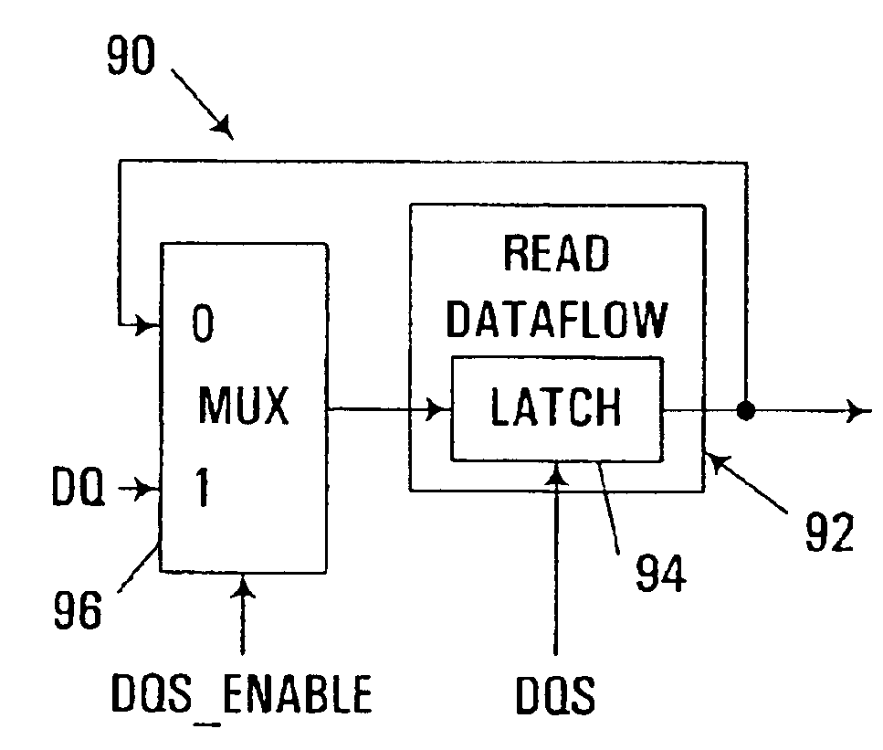
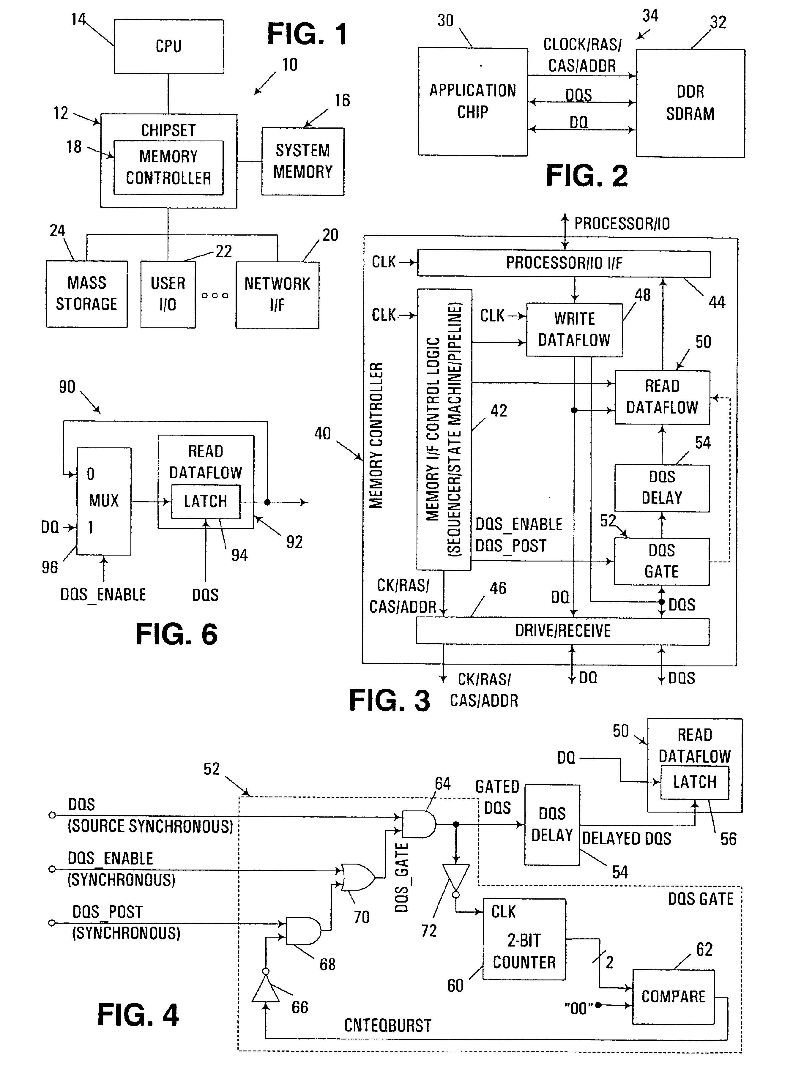
[0015]The invention addresses these and other problems associated with the prior art by providing a circuit arrangement and method for use in connection with a data latch that is coupled to a data source over a source synchronous communications interface. The circuit arrangement and method, in particular, disable the data latch from latching data from the data source whenever the data source is not driving the source synchronous data strobe signal. As such, when the data source is not driving the source synchronous data strobe signal, undesired and / or inadvertent latching by the data latch can be avoided. Moreover, in implementations where a data strobe signal line is bidirectional, and capable of being driven either by the data source or by another circuit used to access the data source (e.g., a memory controller), disabling data latching as described herein can minimize the risk of driver damage resulting from conflicting attempts to drive the data strobe signal line at both ends.

Problems solved by technology

As computers and computer processors increase in performance, memory access performance becomes a significant bottleneck on overall system performance.
The interface technology utilized to communicate data between a memory device and memory controller or other form of application device in particular can be a significant source of such a bottleneck.
The bidirectionality of the data and data strobe lines, however, can raise significant data integrity and reliability concerns.
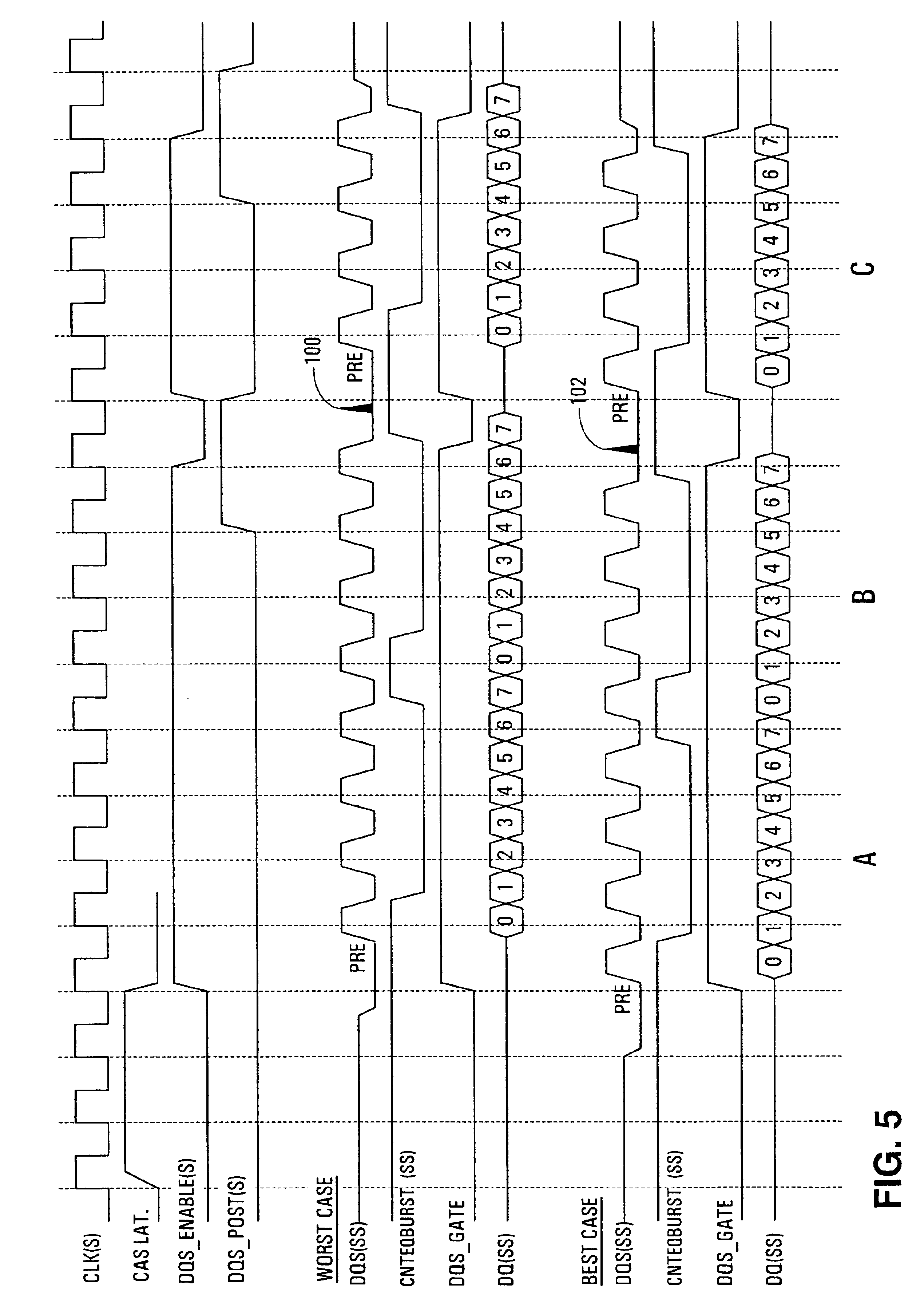
In particular, it is often difficult to manage the control over a data strobe line to ensure that an appropriate data strobe signal is driven at the appropriate times and by the appropriate device, and without any undesired transitions, or “glitches” on the line.
Such inadvertent latchings may produce data integrity problems, which at the best may reduce performance due to the need to repeat a faulty memory transfer operation, or at the worst may corrupt the data utilized by a data processing system.
However, as SDRAM interfaces are driven at higher speeds, control over the data strobe signal becomes a comparatively bigger problem, often resulting in more glitches on the data strobe line.
Moreover, signal skew variations may make it difficult to ensure that only one source drives the data strobe signal at a time, often due to the inability to predict accurately whether a device coupled to the other end of the interface is going to be driving the data strobe signal.
In this context, conventional manners of minimizing glitches on a data strobe signal line are inadequate.
First, utilizing a memory controller to drive the data strobe line low when the line is not being used presents a significant risk of damaging or destroying the driver circuits on either or both of the memory controller and the SDRAMs.
Should both the memory controller and SDRAM attempt to drive the data strobe line simultaneously at different levels, excessive current would typically be generated across the line, and potentially damage or destroy the driver circuitry on either or both devices.
Second, the use of a pull down resistor is also not compatible with high speed operation, since the additional delays due to additional capacitance, current and wiring associated with the pull down resistor can restrict the maximum operating frequency of the interface.
Thus, delays from the memory controller to the SDRAM, coupled with delays back to the memory controller when the SDRAM is performing the data transfer (which can vary from device to device due to process variations), make it difficult to predict the total amount of skew that will occur in the system.
Nonetheless, similar problems as discussed above may be associated with write operations, as well as in source synchronous interfaces other than SDRAM interfaces.

Method used


Image

  • Data strobe gating for source synchronous communications interface
  • Data strobe gating for source synchronous communications interface
  • Data strobe gating for source synchronous communications interface

Examples


Embodiment Construction

[0023]The embodiments discussed herein minimize the adverse effects of glitches or other indeterminate states on a data strobe signal in a source synchronous communications interface by gating a data latch on a target device to disable latching whenever a data source is not driving the data strobe signal. In the context of the invention, a source device refers to the device coupled to a source synchronous communications interface that is driving the data strobe and data signals during a data transfer, while a target device refers to the device that is attempting to receive and capture, or latch, one or more data signals responsive to the data strobe signal. Given that a source synchronous communications interface may be bidirectional, it will be appreciated that a particular device may function at different times as either a source or a target consistent with the invention.

[0024]The embodiments discussed hereinafter focus on an implementation of the invention in a synchronous dynami...


PUM


Abstract

A circuit arrangement and method are used in connection with a data latch that is coupled to a data source over a source synchronous communications interface to disable the data latch from latching data whenever the data source is not driving the source synchronous data strobe signal. As such, when the data source is not driving the source synchronous data strobe signal, undesired and / or inadvertent latching by the data latch can be avoided. Moreover, in implementations where a data strobe signal line is bidirectional, and capable of being driven either by the data source or by another circuit used to access the data source (e.g., a memory controller), disabling data latching as described herein can minimize the risk of driver damage resulting from conflicting attempts to drive the data strobe signal line at both ends.

Description

CROSS-REFERENCE TO RELATED APPLICATION[0001]This application is a divisional of U.S. patent application Ser. No. 09 / 836,651, filed on Apr. 17, 2001 now U.S. Pat. No. 6,671,211 by John Michael Borkenhagen et al. and entitled “DATA STROBE GATING FOR SOURCE SYNCHRONOUS COMMUNICATIONS INTERFACE,” the disclosure of which is incorporated by reference herein.FIELD OF THE INVENTION[0002]The invention is generally related to data transmission over source synchronous communications interfaces, e.g., as with synchronous dynamic random access memory (SDRAM) memory interfaces.BACKGROUND OF THE INVENTION[0003]As computers and computer processors increase in performance, memory access performance becomes a significant bottleneck on overall system performance. The interface technology utilized to communicate data between a memory device and memory controller or other form of application device in particular can be a significant source of such a bottleneck.[0004]For dynamic random access memory (DRA...

Claims


Application Information

Patent Timeline
IPC IPC(8): G11C7/10
CPCG11C7/1078G11C7/1087G11C7/109
Inventor BORKENHAGEN, JOHN MICHAELGREENFIELD, TODD ALANMARCELLA, JAMES ANTHONY
Owner IBM CORP
Learn More