Device and method for correcting the duty cycle of a clock signal

Active Publication Date: 2005-09-13
POLARIS INNOVATIONS
View PDF7 Cites 24 Cited by
  • Summary
  • Abstract
  • Description
  • Claims
  • Application Information

AI Technical Summary

Problems solved by technology

The determination of the duty cycle is, in particular with frequencies of e.g. 300 MHz and above, very difficult since with such high frequencies the time difference between the H-level duration th and the L-level duration t1 may be in the range of some Pico seconds.
Thus, the current sources and switches have to be manufactured in a relatively expensive manner, i.e. by making use of a relatively large lay

Method used


Image

  • Device and method for correcting the duty cycle of a clock signal
  • Device and method for correcting the duty cycle of a clock signal
  • Device and method for correcting the duty cycle of a clock signal

Examples


Embodiment Construction

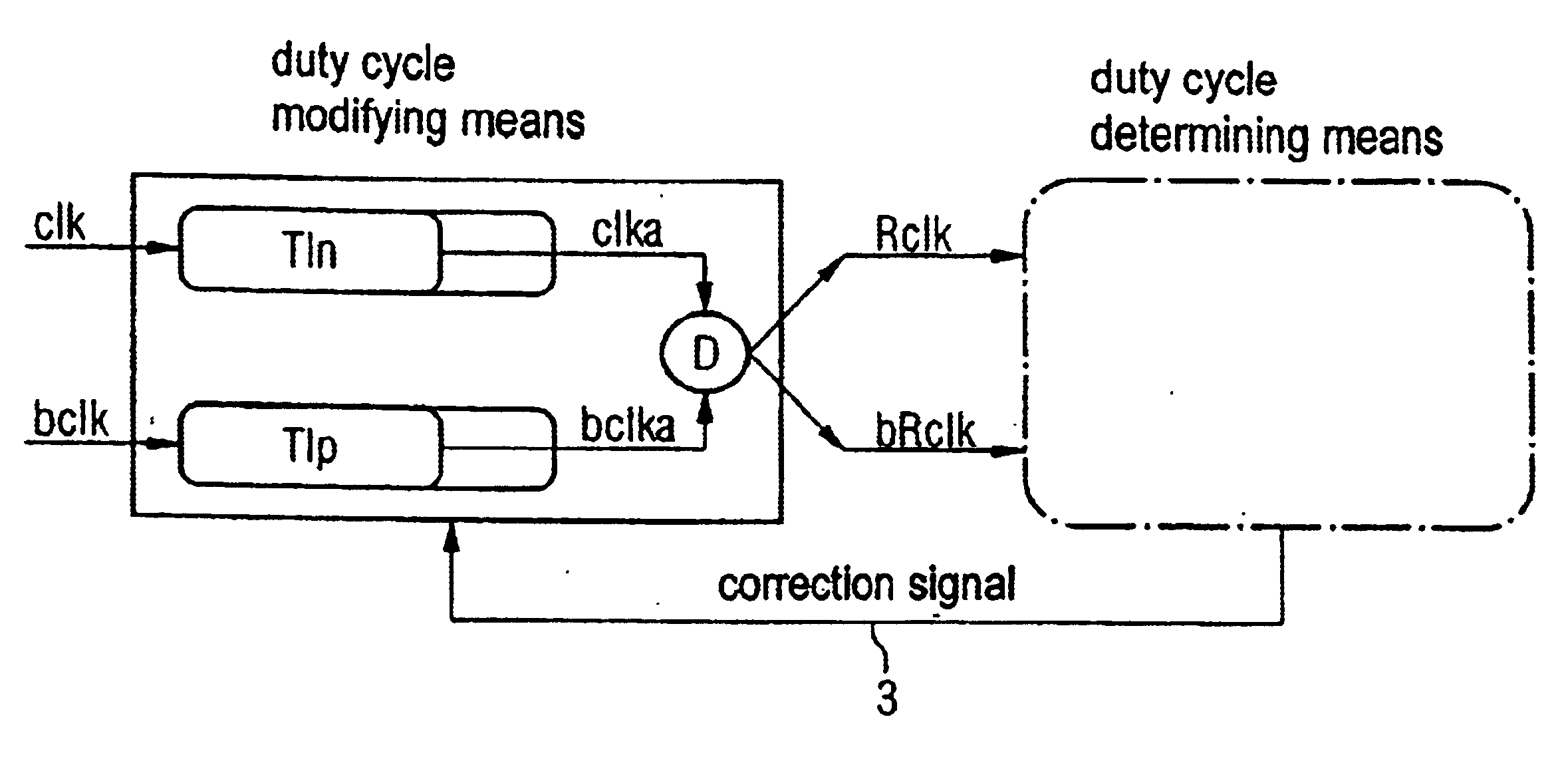
[0024]FIG. 6 illustrates a block diagram of an embodiment of a device for correcting the duty cycle of a clock signal in accordance with the invention. The device according to the invention comprises a duty cycle modifying device illustrated on the left in FIG. 6, and a duty cycle determining means illustrated schematically as a block on the right in FIG. 6.

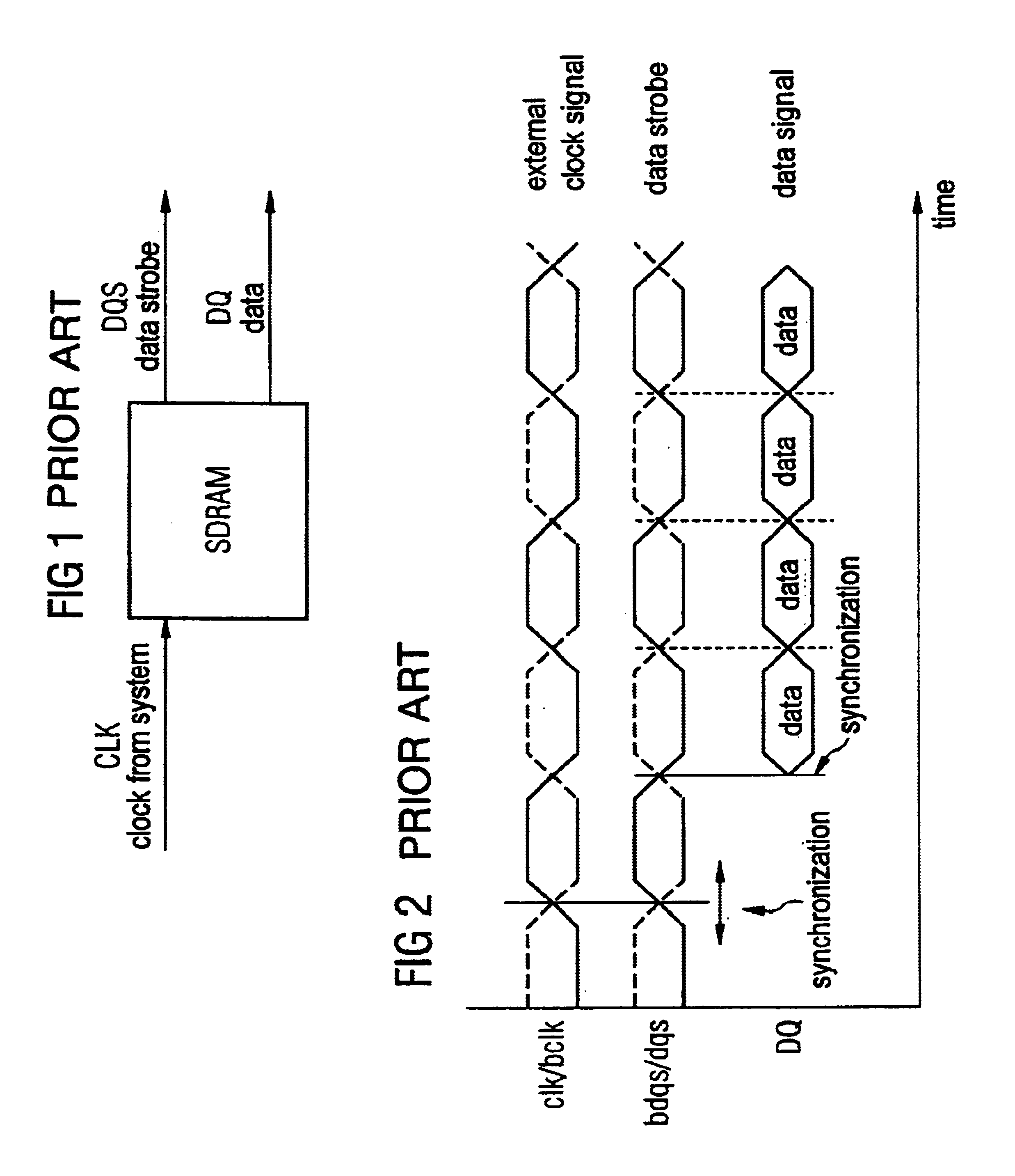
[0025]The duty cycle modifying device used with the described embodiment is known from prior art and has already been described above, so that it will be dealt with only briefly here. The duty cycle modifying device receives, from outside the chip on which the device for correcting the duty cycle of a clock signal in accordance with the invention is located, an external clock signal CLK and a clock signal BCLK complementary thereto. These clock signals may, for instance, be received by a chip that is connected with the chip on which the device in accordance with the invention is located. The external chip which will, to simplify ...


PUM


Abstract

A device for correcting the duty cycle of a clock signal with a duty cycle modifying device which receives a clock signal and a complementary clock signal, which comprises a delay device for both clock signals, and which is adapted to generate a clock signal and a complementary clock signal with corrected duty cycle. The invention also relates to a corresponding method for correcting the duty cycle of a clock signal and may preferably be used to correct the duty cycle of the system clock input in a DDR-SDRAM device in order that an ideal duty cycle of 50 percent is achieved in the memory chip during the processing thereof to a data strobe. As compared to previous similar devices and methods, the invention thus enables, with DDR-SDRAM devices, a more precise reading out of the data from the devices to the system associated with the devices.

Description

CLAIM FOR PRIORITY[0001]This application claims the benefit of priority to German Application No. 103 20 794.5, filed in the German language on Apr. 30, 2003, the contents of which are hereby incorporated by reference.TECHNICAL FIELD OF THE INVENTION[0002]The present invention relates to a device and a method for correcting the duty cycle of a clock signal.BACKGROUND OF THE INVENTION[0003]Synchronous dynamic semiconductor memories with random access (SDRAM), and in particular SDRAM with double data rate (DDR-SDRAM) output, during reading out, their data (for which the abbreviation “DQ” is used) synchronously to a clock signal output by the memory. This clock signal, which is also referred to as data strobe and is usually abbreviated as “DQS”, in turn has to be synchronous to a clock signal (CLK) input externally in the memory. The external clock signal is generated by devices connected with the memory and communicating therewith and conveying the read instruction to the memory, said...

Claims


Application Information

Patent Timeline
IPC IPC(8): G11C7/10G11C7/00G11C7/22G11C11/4076G11C11/407H03K5/156
CPCG11C7/1072G11C7/22G11C7/222G11C11/4076H03K5/1565
Inventor MINZONI, ALESSANDRO
Owner POLARIS INNOVATIONS
Why Eureka
Try Eureka