Low voltage data path and current sense amplifier

a data path and low-voltage technology, applied in the field of data paths in memory devices, can solve the problems of low internal voltage level, data path b>100/b> may not consistently or accurately sense data read from memory cell arrays, and read errors occur

Active Publication Date: 2005-09-13
MICRON TECH INC
View PDF19 Cites 34 Cited by
  • Summary
  • Abstract
  • Description
  • Claims
  • Application Information

AI Technical Summary

Benefits of technology

[0014]A data path according to one embodiment of the present invention couples read data from a read / write circuit to an output buffer. The data path includes a local input / output (LIO) line coupled to the read / write circuit and an input / output (IO) line coupling circuit having first and second control terminals coupled to first and second signal lines of the LIO line. The coupling circuit has a supply terminal coupled to an internal voltage supply, and first and second output nodes to which the supply terminal is coupled and from which the supply terminal is decoupled according to the complementary data coupled to the first and second signal lines of the LIO line. The data path further includes a global input / output (GIO) line coupled to the output terminals of the IO line coupling circuit and further coupled to an output data amplifier for generating complementary output voltage signals based on input currents coupled over the GIO line to the output data amplifier.

Problems solved by technology

Conventional current mode data paths, such as the data path 100, however, suffer when operated at low internal voltage levels.
However, where it is desirable to implement the data path 100 under operating conditions having voltage levels approaching 1.0 volts, the data path 100 may not consistently or accurately sense data read from the memory cell array 104.
As a result, a read error occurs.

Method used


Image

  • Low voltage data path and current sense amplifier
  • Low voltage data path and current sense amplifier
  • Low voltage data path and current sense amplifier

Examples


Embodiment Construction

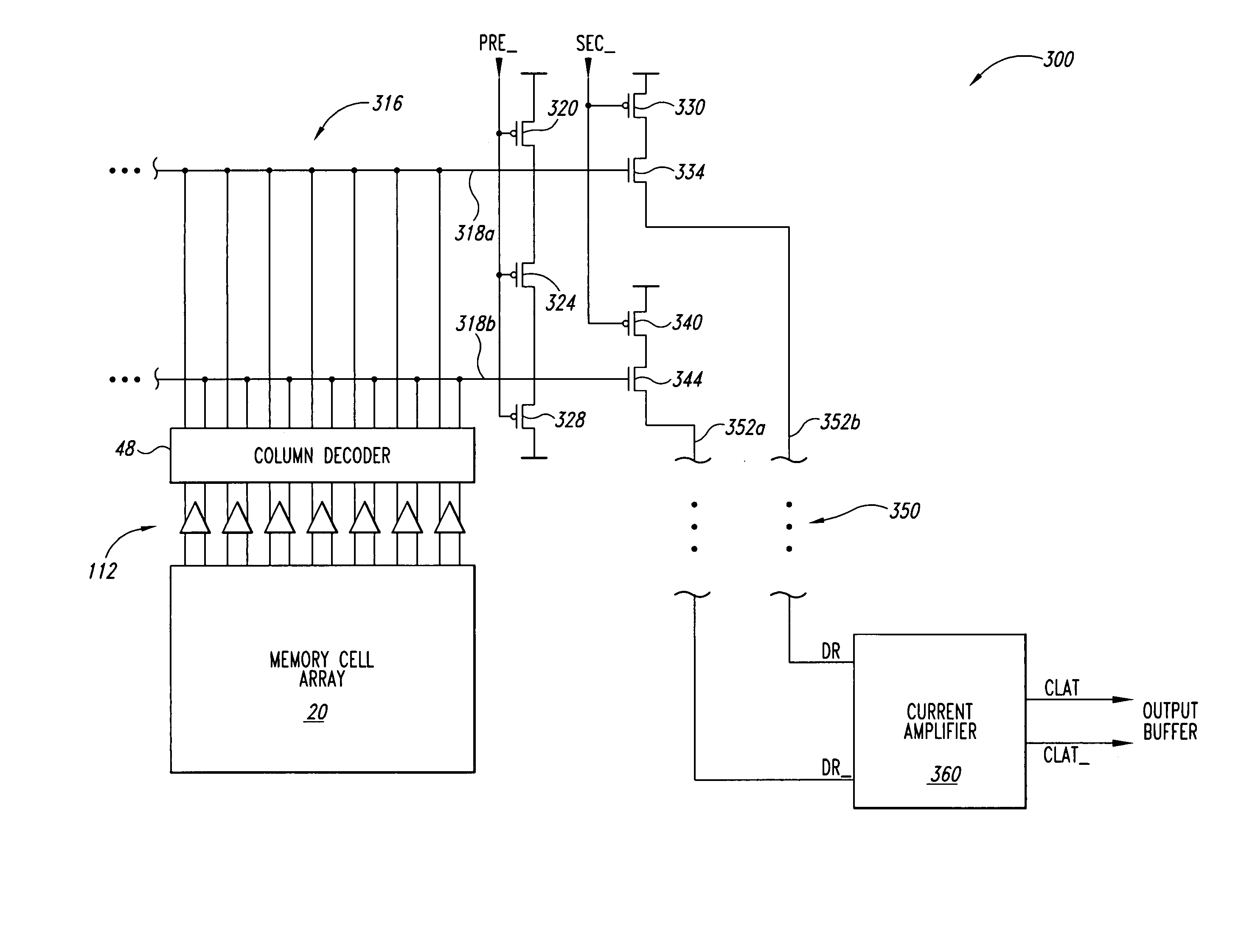
[0022]FIG. 3 illustrates a data path 300 according to an embodiment of the present invention. The data path 300 can be operated under low voltage conditions, such as in memory devices designed for low voltage operation. Certain details are set forth below to provide a sufficient understanding of the invention. However, it will be clear to one skilled in the art that the invention may be practiced without these particular details. In other instances, well-known circuits, control signals, timing protocols, and software operations have not been shown in detail in order to avoid unnecessarily obscuring the invention.

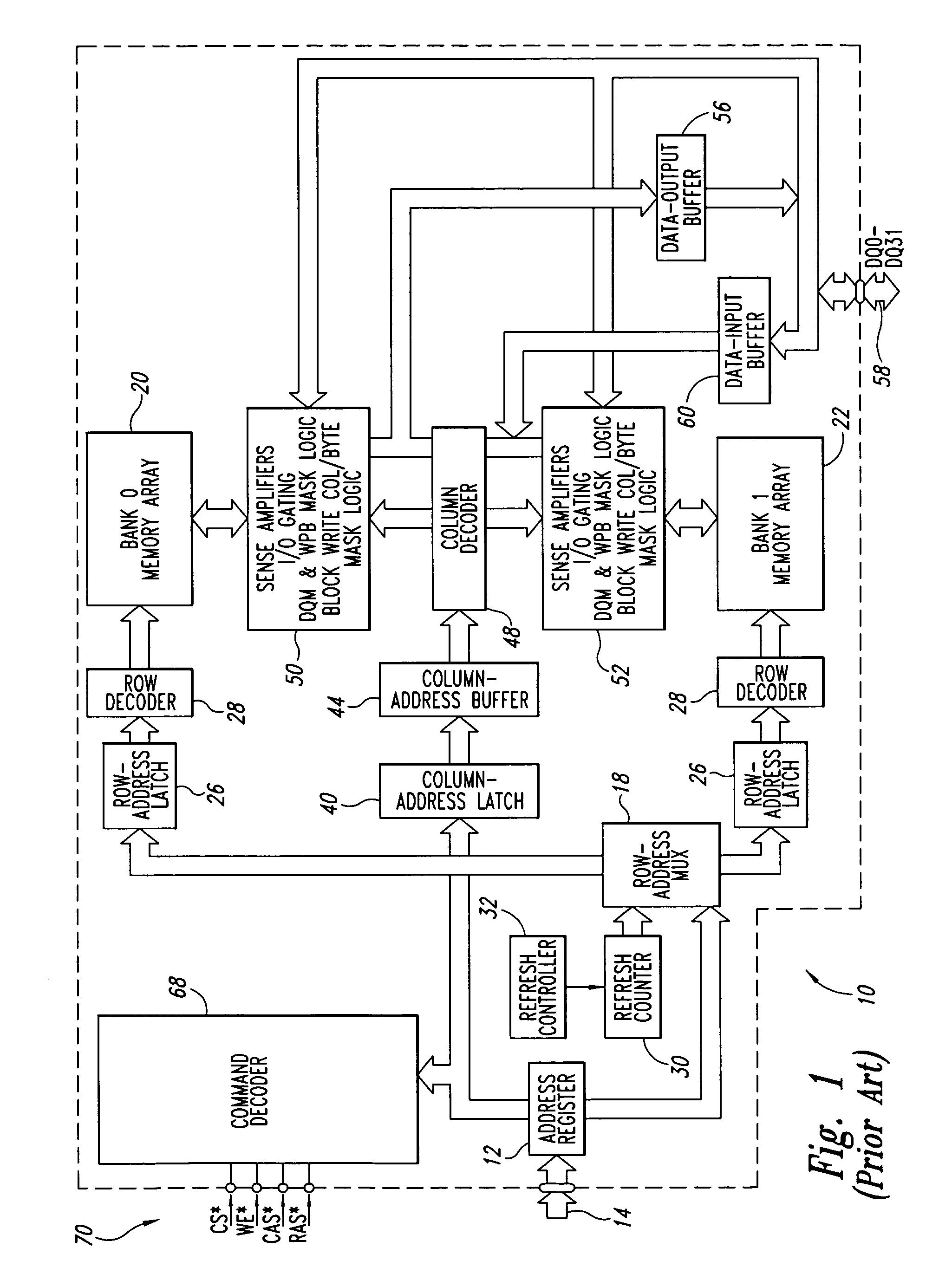
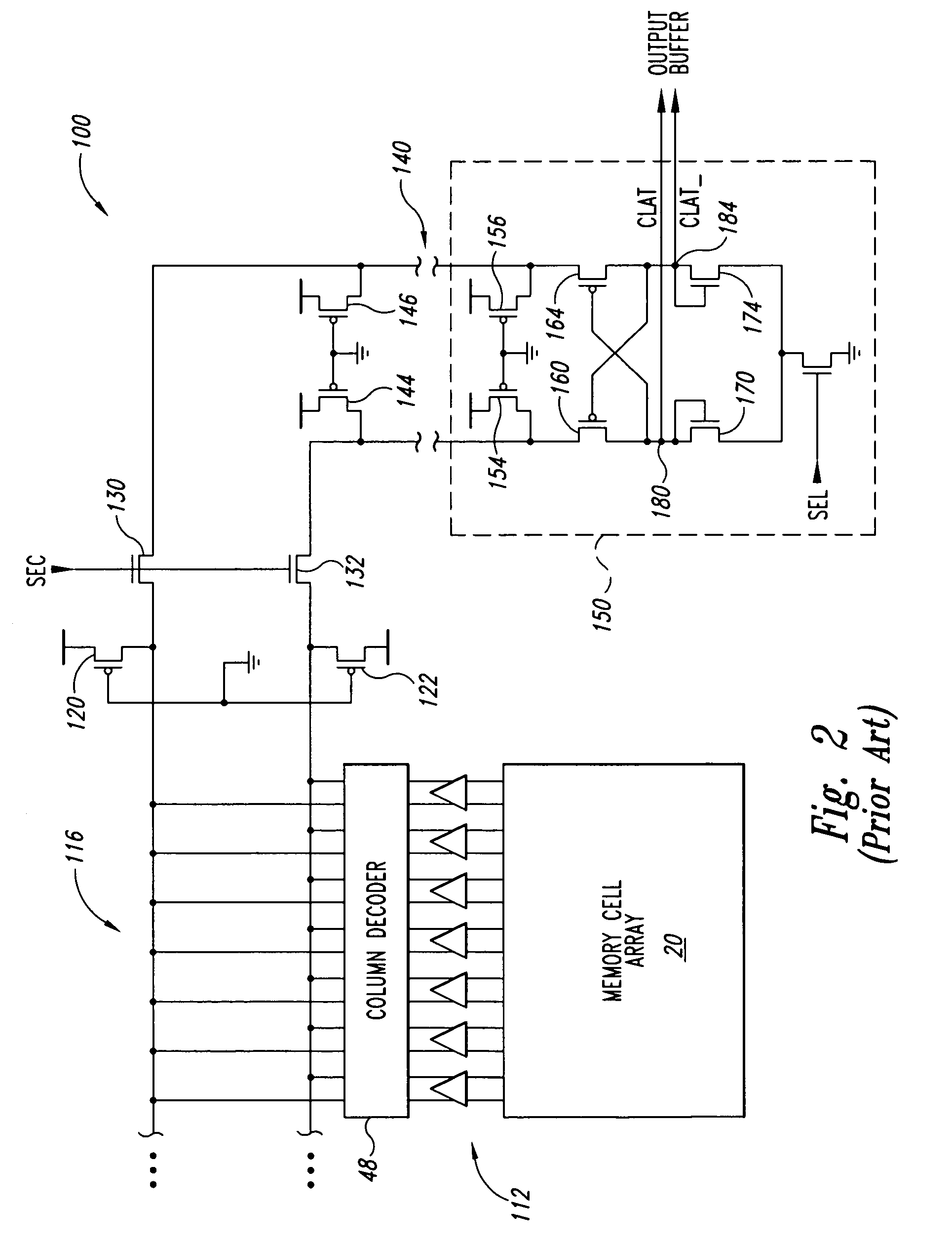
[0023]The data path 300 includes elements similar to the data path 100 (FIG. 2), and where appropriate, the same reference number is used to refer to the same element. The data path 300 is coupled through the column decoder 48 and sense amplifiers 112 to the memory cell array 20, which is arranged in rows and columns of memory cells. The column decoder 48 selectively couples...


PUM


Abstract

A data path including a local input/output (LIO) line and a global input/output (GIO) line coupled together through an input/output (IO) line coupling circuit. The coupling circuit is coupled to an internal voltage supply, and couples and decouples signal lines of the GIO line from the supply terminal according to read data coupled to the LIO line. The GIO line is coupled to a current sense amplifier to generate output voltage signals that are coupled to an output buffer. An example of a current sense amplifier coupled to the GIO line includes first and second load circuits and first and second n-channel MOS (NMOS) transistors coupled to a respective load circuit. The gates of NMOS transistors are cross coupled, and input current signals are coupled to source terminals of the NMOS transistors and the output voltage signals are coupled from the drain terminals of the NMOS transistors.

Description

TECHNICAL FIELD[0001]The invention relates generally to integrated circuit memory devices, and more particularly, to a data path in a memory device.BACKGROUND OF THE INVENTION[0002]As the processing speed of microprocessors increases, the demand for memory devices having faster access times also increases. Additionally, the demand for memory devices that are designed for low voltage operation has also increased with the popularity of portable computing devices, which are typically battery operated. Memory system designers have developed methods and designs that shave off nanoseconds from access times in order to satisfy the demand for high speed memory devices while operating under low voltage conditions. Even with the advances made in memory device designs, the fundamental building blocks of memory devices have remained relatively the same. As will be described in more detail below, these building blocks are the basic elements that are shared among all types of memory devices, rega...

Claims


Application Information

Patent Timeline
Patent Type & Authority Patents(United States)
IPC IPC(8): G11C7/00
CPCG11C7/062G11C7/18G11C2207/063
Inventor JING, CHUL MIN
Owner MICRON TECH INC
Why Eureka
Try Eureka