Skew adjusting circuit and semiconductor integrated circuit

a technology of semiconductor integrated circuits and skews, which is applied in the direction of generating/distributing signals, instruments, recording signal processing, etc., can solve the problems of troublesome adjustment of skews using a measuring device, affecting the timing and supply of a plurality of nodes, and affecting the timing of skews of node outputs

a technology of semiconductor integrated circuits and skews, which is applied in the direction of generating/distributing signals, instruments, recording signal processing, etc., can solve the problems of troublesome adjustment of skews using a measuring device, affecting the timing and supply of a plurality of nodes, and affecting the timing of skews of node outputs

US6944801B2Inactive Publication Date: 2005-09-13NEC CORP

Image

  • Skew adjusting circuit and semiconductor integrated circuit
  • Skew adjusting circuit and semiconductor integrated circuit
  • Skew adjusting circuit and semiconductor integrated circuit

Examples


Embodiment Construction

[0027]Next, with reference to the accompanying drawings, an embodiment of the present invention will be described.

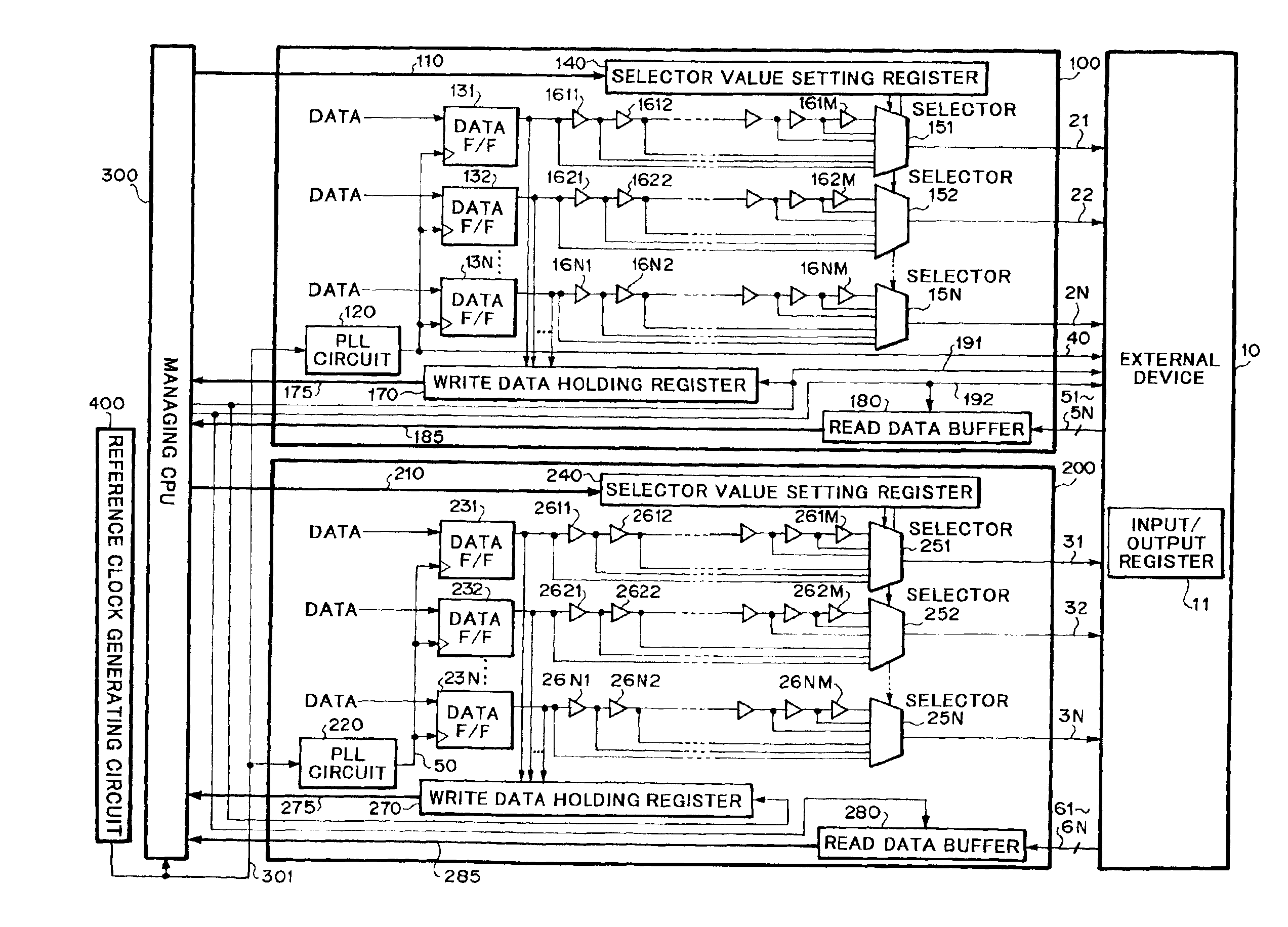
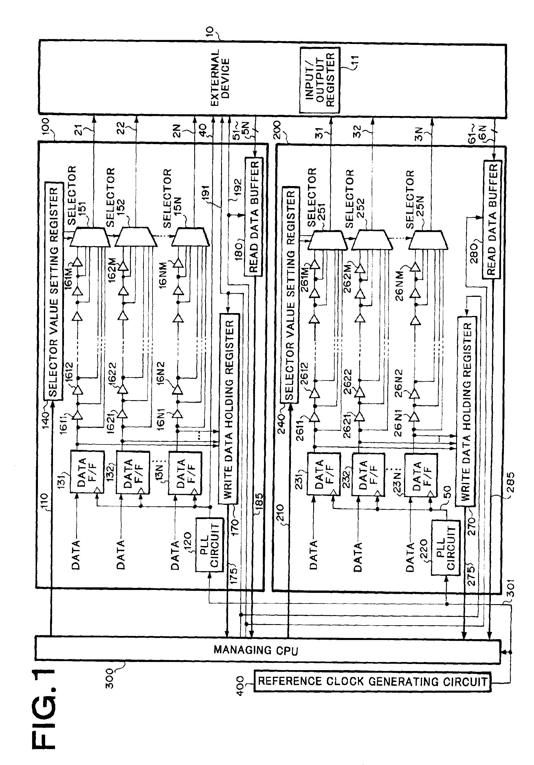
[0028]Referring to FIG. 1, the system according to the embodiment of the present invention has an external device 10, a managing CPU 300, and nodes 100 and 200.

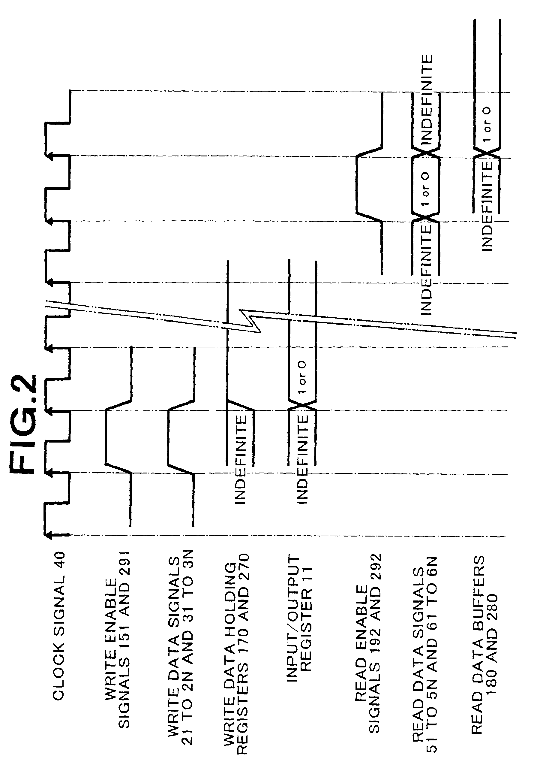
[0029]The external device 10 inputs write data signals 21, 22, . . . , and 2N from the node 100. In addition, the external device 10 inputs write data signals 31, 32, . . . , and 3N from the node 200. The external device 10 stores these input signals to an input / output register 11. The write data signals 21, 22, . . . , and 2N synchronize with a clock signal 40 that a PLL circuit 120 of the node 100 generates. The write data signals 31, 32, . . . , and 3N synchronize with a clock signal 50 that a PLL circuit 220 of the node 200 generates. In this example, the PLL circuit 120 multiplies the frequency of a reference clock signal 301 that a reference clock generating circuit 400 generates so as to generate the clock ...


PUM


Abstract

An output signal of a flip flop at an output stage is supplied to delay gates connected in series thereto. A selector selects the output signal of the flip flop at the output stage or an output signal of one of the delay gates and supplies the selected signal to an external device. A signal to be selected by the selector depends on the value of data stored in a selector value setting register. When a skew adjustment is performed, the output signal of the flip flop at the output stage is held in a write data holding register. The signal supplied to the external device is held in a read data buffer through an input / output register of the external device. Until the value of the signal stored in the write data holding register matches the value of the signal held in the read data buffer, the value of the data stored in the selector value setting register is varied.

Description

BACKGROUND OF THE INVENTION[0001]1. Field of the Invention[0002]The present invention relates to a skew adjusting circuit, and in particular, to a skew adjusting circuit for adjusting a skew of a data signal supplied from a semiconductor integrated circuit to an external device against a clock.[0003]2. Description of the Prior Art[0004]In a system that has a plurality of nodes (each of which is composed of an IC), an external device, and a managing CPU that manages the operations and states of the plurality of nodes, when clock signals and data signals are supplied from the plurality of nodes to the external device, it may be necessary to adjust skews of signals between the plurality of nodes and the external device.[0005]In recent years, since the widths of data buses for CPUs, peripheral circuits, and so forth are becoming large, the number of lines for data bit signals contained in data buses is increased. Thus, it is difficult to route all data bit lines in the same length. Cons...

Claims


Application Information

Patent Timeline
13 Sep 2005
Publication
US6944801B2
IPC
H03K19/003; G06F13/42; G06F1/12; H04L7/00
CPC
H03K19/00323
Inventors
KOJIMA, TAKASHI