Photovoltaic devices fabricated by growth from porous template

a technology of photovoltaic devices and porous templates, applied in thermoelectric devices, sustainable manufacturing/processing, final product manufacturing, etc., can solve the problems of reducing the hole and electron transport efficiency, interim recombination loss, and uncontrollable active layer morphology

Inactive Publication Date: 2005-09-20
AERIS CAPITAL SUSTAINABLE IP
View PDF23 Cites 204 Cited by
  • Summary
  • Abstract
  • Description
  • Claims
  • Application Information

AI Technical Summary

Problems solved by technology

In these solar cell devices, however, the device architectures are suboptimal in terms of their nanometer-scale morphology, and improvements are needed to obtain higher-efficiency devices.
For instance, in the Huynh et al. work, the nanorods are sprinkled across the polymer in which they are embedded; they often cluster into clumps of nanorods, producing some areas with more nanorods than ideal and other areas with fewer nanorods than ideal; and not all nanorods are fully connected so that islands may exists where charges are trapped (and even if full connectivity exists, charges generally cannot move out of the cell in a simple straight path, with interim recombination losses resulting).
In the polymer-blend work of Schmidt-Mende and others, phase separation leads to a morphology of the active layer that is not well controlled, with islands and percolation paths that are not straight.
Finally, in devices of the prior art, the movement of charges through the active materials of the devices required regularly and closely spaced nanoparticles or nanorods which could collect and transport free electrons to the outer boundary of the active layer of the device, and the lack of uniform spacing in these devices decreased the hole and electron transport efficiency.
All of these factors combine to reduce the device efficiency, and therefore the potential electricity that can be produced by a solar cell.
Finally, devices of the prior art link materials choice with architecture, making it hard to optimize materials independent of shape.

Method used


Image

  • Photovoltaic devices fabricated by growth from porous template
  • Photovoltaic devices fabricated by growth from porous template
  • Photovoltaic devices fabricated by growth from porous template

Examples


Embodiment Construction

Contents

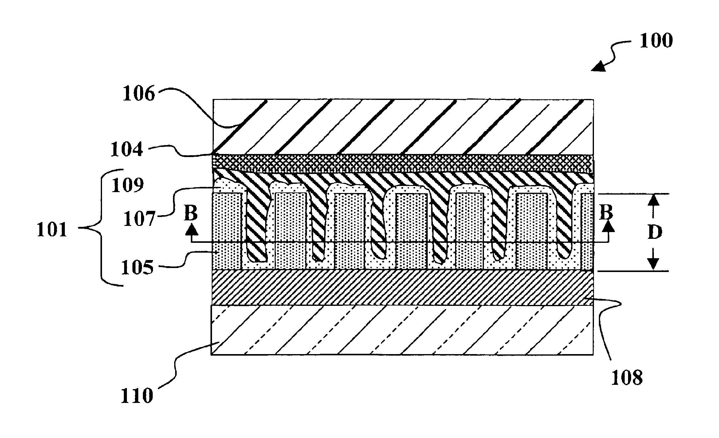
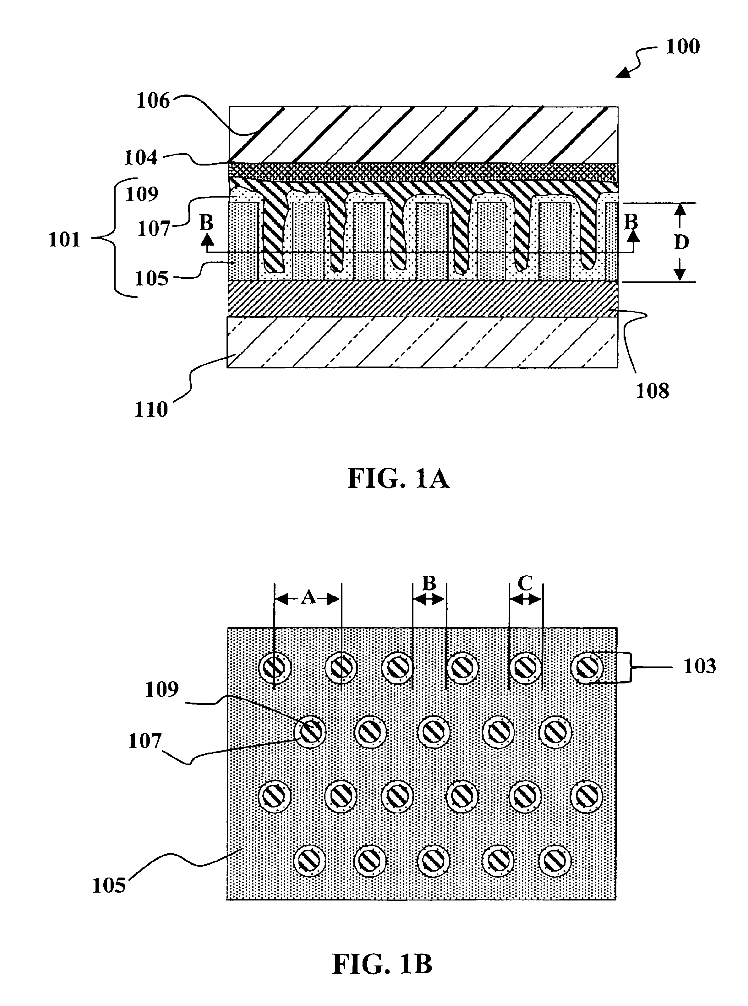
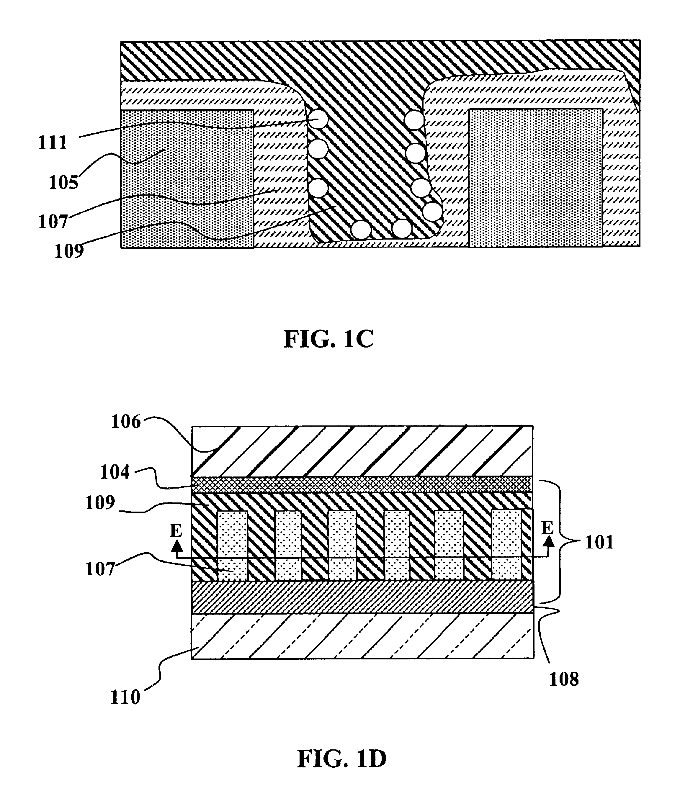
[0024]I. Glossary[0025]II. Introduction[0026]III. General Overview[0027]IV. Photovoltaic Device[0028]V. Photovoltaic Device Fabrication[0029]VI. Alternative Embodiments[0030]VII. Conclusion

I. Glossary

[0031]The following terms are intended to have the following general meanings as they are used herein:

[0032]The article “A”, or “An” refers to a quantity of one or more of the item following the article, except where expressly stated otherwise, e.g., “a single” layer.

[0033]Active Layer generally refers to the layer within a photovoltaic or solar cell device where conversion of radiant energy to electrical energy takes place.

[0034]Anodization refers to the formation of a film, such as an oxide, on a conducting material, such as a metal, by electrolysis.

[0035]Array refers to a regular arrangement of objects or structures over a scale of distance greater than some characteristic dimension of a typical structure or object in the array.

[0036]Aspect Ratio: refers to the ratio of pore ...


PUM

PropertyMeasurementUnit
distancesaaaaaaaaaa
distancesaaaaaaaaaa
diameteraaaaaaaaaa

Abstract

Photovoltaic devices, such as solar cells, and methods for their manufacture are disclosed. A device may be characterized by an architecture where two more materials having different electron affinities are regularly arrayed such that their presence alternates within distances of between about 1 nm and about 100 nm. The materials are present in a matrix based on a porous template with an array of template pores. The porous template is formed by anodizing a layer of metal. A photovoltaic device may include such a porous template disposed between a base electrode and a transparent conducting electrode. A first charge-transfer material fills the template pores, A second (complementary) charge-transfer material fills additional space not occupied by the first charge-transfer material.

Description

CROSS-REFERENCE TO RELATED APPLICATIONS[0001]This application is a continuation-in-part of U.S. patent application Ser. No. 10 / 290,119 filed Nov. 5, 2002, and is a continuation-in-part of U.S. patent application Ser. No. 10 / 303,665 filed Nov. 22, 2002, and is a continuation-in-part of U.S. patent application Ser. No. 10 / 319,406 filed Dec. 11, 2002, the entire disclosures of all of which are incorporated herein by reference. This application also claims priority to U.S. Provisional Patent Application 60 / 390,904, filed Jun. 22, 2002, the entire disclosures of which are incorporated herein by reference.FIELD OF THE INVENTION[0002]This invention is directed to photovoltaic devices and methods for their production, and more specifically to nanostructured photovoltaic devices.BACKGROUND OF THE INVENTION[0003]In the prior art, inexpensive plastic solar cells based on exciton (bound electron / hole pairs) physics have been fabricated with AM1.5 efficiency of 2-3% (Huynh et al., “Hybrid Nanoro...

Claims


Application Information

Patent Timeline
Patent Type & Authority Patents(United States)
IPC IPC(8): H01L31/0352H01L31/0248H01L31/0256H01L31/00H01LH01L31/042H01L31/18
CPCH01L51/4213H01L51/422H01L51/447H01L51/0036H01L51/0037H01L51/4253Y02E10/549Y02P70/50H10K85/113H10K85/1135H10K30/15H10K30/10H10K30/30H10K30/87
Inventor SAGER, BRIAN M.ROSCHEISEN, MARTIN R.PETRITSCH, KLUSPICHLER, KARLFIDANZA, JACQUELINEYU, DONG
Owner AERIS CAPITAL SUSTAINABLE IP
Why Eureka
Try Eureka