Electronic package with passive components

a passive component and electronic package technology, applied in the field of electronic packages, can solve the problems of increasing the cost of mounting the passive component b>130/b>, the tendency of the neighboring wire to become a short circuit, and the increase of the cost of the passive component. to achieve the effect of enhancing the reliability of the electronic packag

Active Publication Date: 2005-09-20
VIA TECH INC
View PDF2 Cites 33 Cited by
  • Summary
  • Abstract
  • Description
  • Claims
  • Application Information

AI Technical Summary

Benefits of technology

[0013]Accordingly, in an embodiment of the present invention, an electronic package with a passive compon

Problems solved by technology

However, this may cause the wires 160 to be shifted during encapsulating the molding compound 170, so the neighboring wires 160 may be led to become a short circuit.
However, after exposed to the air, the solder paste is

Method used


Image

  • Electronic package with passive components
  • Electronic package with passive components
  • Electronic package with passive components

Examples


first embodiment

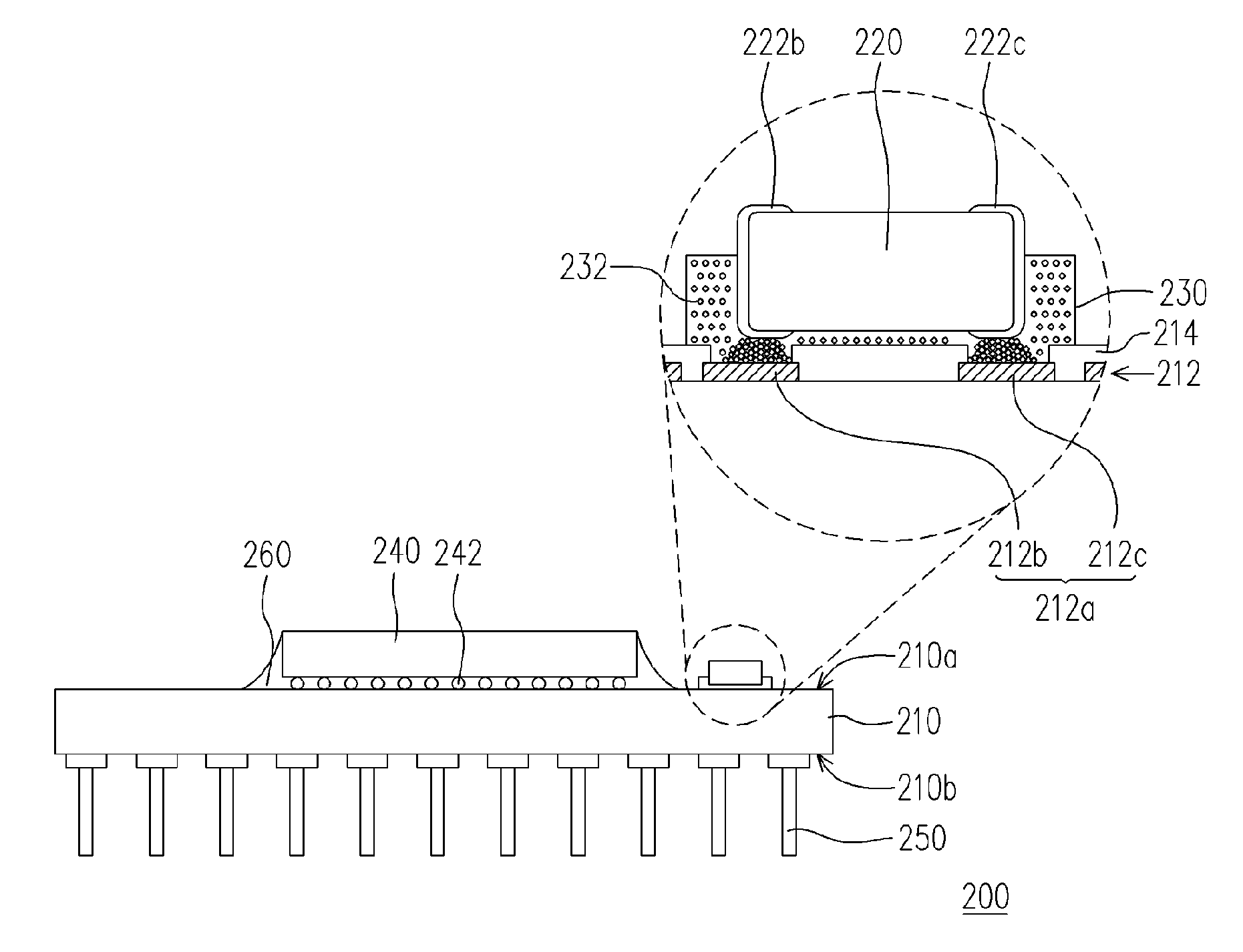
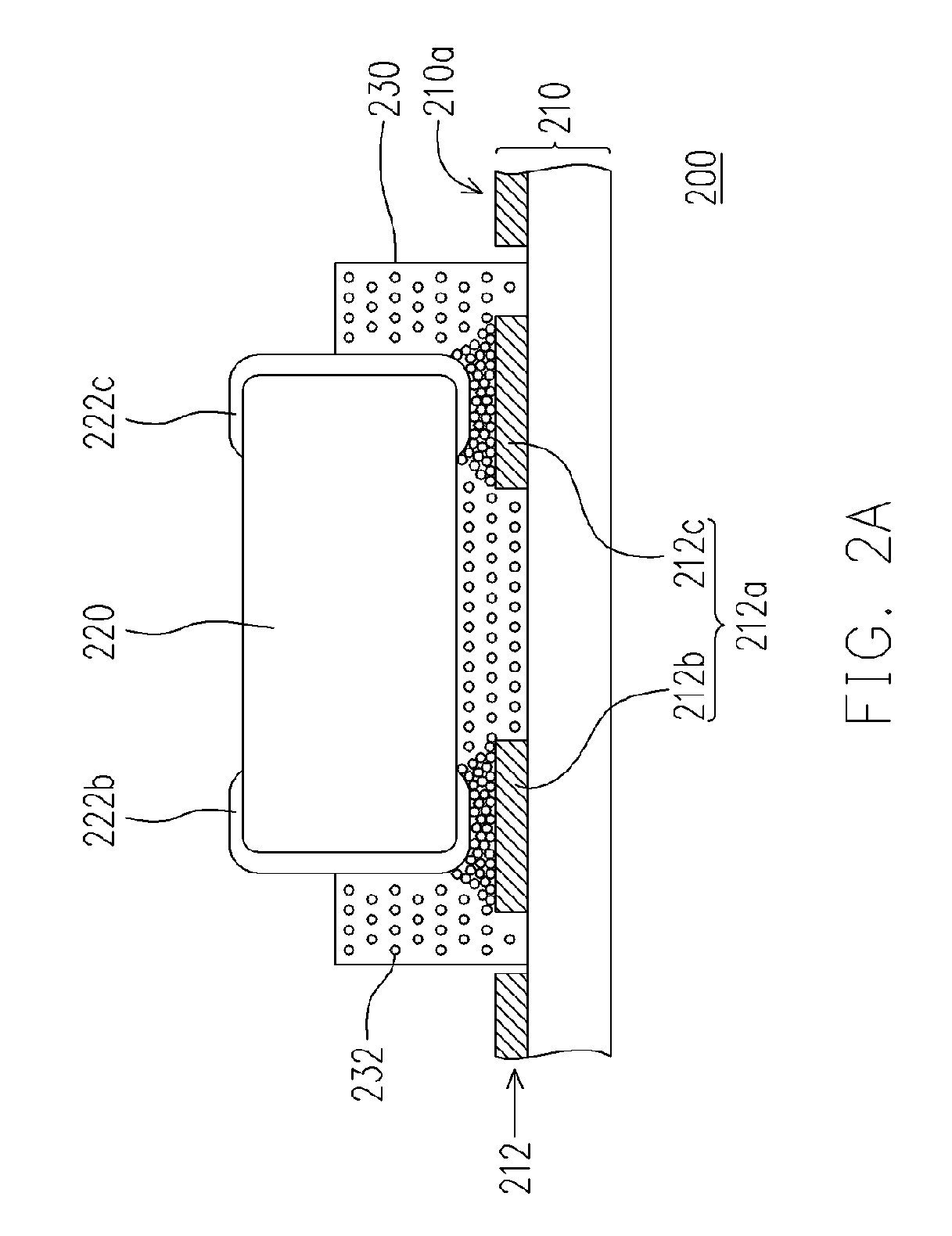
[0024]FIGS. 2A and 2B are cross-sectional views depicting an electronic package with a passive component according to a first embodiment of the present invention. Referring to FIG. 2A, the electronic package 200 includes a circuit carrier 210, at least a passive component 220 and an anisotropic conductive layer 230, wherein the passive component 220 is electrically connected to the circuit carrier 210 through the anisotropic conductive layer 230. The circuit carrier 210 includes a patterning circuit layer 212 formed on a first surface 210a thereof. The patterning circuit layer 212 has at least a passive-component-pad set 212a including a first pad 212b and a second pad 212c. The passive component 220 has a first electrode 222b and a second electrode 222c that are positioned over the first pad 212b and the second pad 212c. The anisotropic conductive layer 230 is deposited between the first electrode 222b and the first pad 212b and between the second electrode 222c and the second pad ...

second embodiment

[0030]FIGS. 3A through 3C are cross-sectional views depicting an electronic package with a passive component according to a second embodiment of the present invention. The same reference numerals used throughout the first embodiment and the second embodiment indicate the same or similar elements.

[0031]Referring to FIG. 3A, the second embodiment is similar to the first embodiment. The difference between the second embodiment and the first embodiment is that the circuit carrier 210 further includes a solder-mask layer 214 formed over the patterning circuit layer 212. The exposed area of the first pad 212b and the second pad 212c is defined by the solder-mask layer 214. The relationship between the pads and the solder-mask layer 214 is termed as solder-mask-defined type (SMD). The anisotropic conductive layer 230 covers the first pad 212b and the second pad 212c and further covers the region between the first pad 212b and the second pad 212c, as shown in FIG. 3A. Alternatively, the ani...


PUM


Abstract

An electronic package with a passive component includes a circuit carrier, at least a passive component and an anisotropic conductive layer. The circuit carrier has at least a passive-component-pad set including multiple pads. The passive component has multiple electrodes placed over the corresponding pads of the passive-component-pad set. The anisotropic conductive layer is deposited between the electrodes and the pads.

Description

CROSS-REFERENCE TO RELATED APPLICATION[0001]This application claims the priority benefit of Taiwan application serial no. 93115225, filed May 28, 2004.BACKGROUND OF THE INVENTION[0002]1. Field of the Invention[0003]The present invention generally relates to an electronic package. More particularly, the present invention relates to an electronic package with a passive component.[0004]2. Description of the Related Art[0005]Passing with the development of electronic technology, electronic products with multiple function are continuously released and have a trend with lightness, thinness, shortness and smallness. A circuit carrier, such as printed circuit board (PCB) or chip carrier, is commonly used in an electronic package. The circuit carrier is mainly composed of multiple patterning circuit layers and multiple dielectric layers that are provided with a stack by turns. The dielectric layer is deposited between the neighboring patterning circuit layers. Multiple plated through holes o...

Claims


Application Information

Patent Timeline
IPC IPC(8): H01L23/28H05K5/06H01L21/60H01L25/16H05K3/28H05K3/32H05K3/34
CPCH01L25/16H05K3/323H01L2224/16H05K2201/10636H05K3/3452H01L2224/32225H01L2224/48091H01L2224/48227H01L2224/73265H01L2924/01078H01L2924/15311H01L2924/15312H01L2924/19041H01L2924/19105H05K3/284H01L2924/00014H01L2924/00H01L2924/00012H01L24/73Y02P70/50
Inventor LEE, I-TSENGTSENG, JEN-TE
Owner VIA TECH INC
Why Eureka
Try Eureka