Resistance random access memory

a random access memory and resistance technology, applied in the field of resistive random access memory (“ rram”), can solve the problems of inability to erase or reset data in the memory device after being programmed, and the size of type 1r1t rram is too big

Inactive Publication Date: 2005-09-20
WINBOND ELECTRONICS CORP
View PDF13 Cites 89 Cited by
  • Summary
  • Abstract
  • Description
  • Claims
  • Application Information

AI Technical Summary

Benefits of technology

[0011]An object of the present invention is to provide a resistance random access memory and method of fabricating the same to make Type 1R1T RRAM erasable and programmable.

Problems solved by technology

However, the size of Type 1R1T RRAM is too big.
Because the diode only allows to be turned on in one direction, the data in the memory device cannot be erased or reset after being programmed.

Method used


Image

  • Resistance random access memory
  • Resistance random access memory
  • Resistance random access memory

Examples


Embodiment Construction

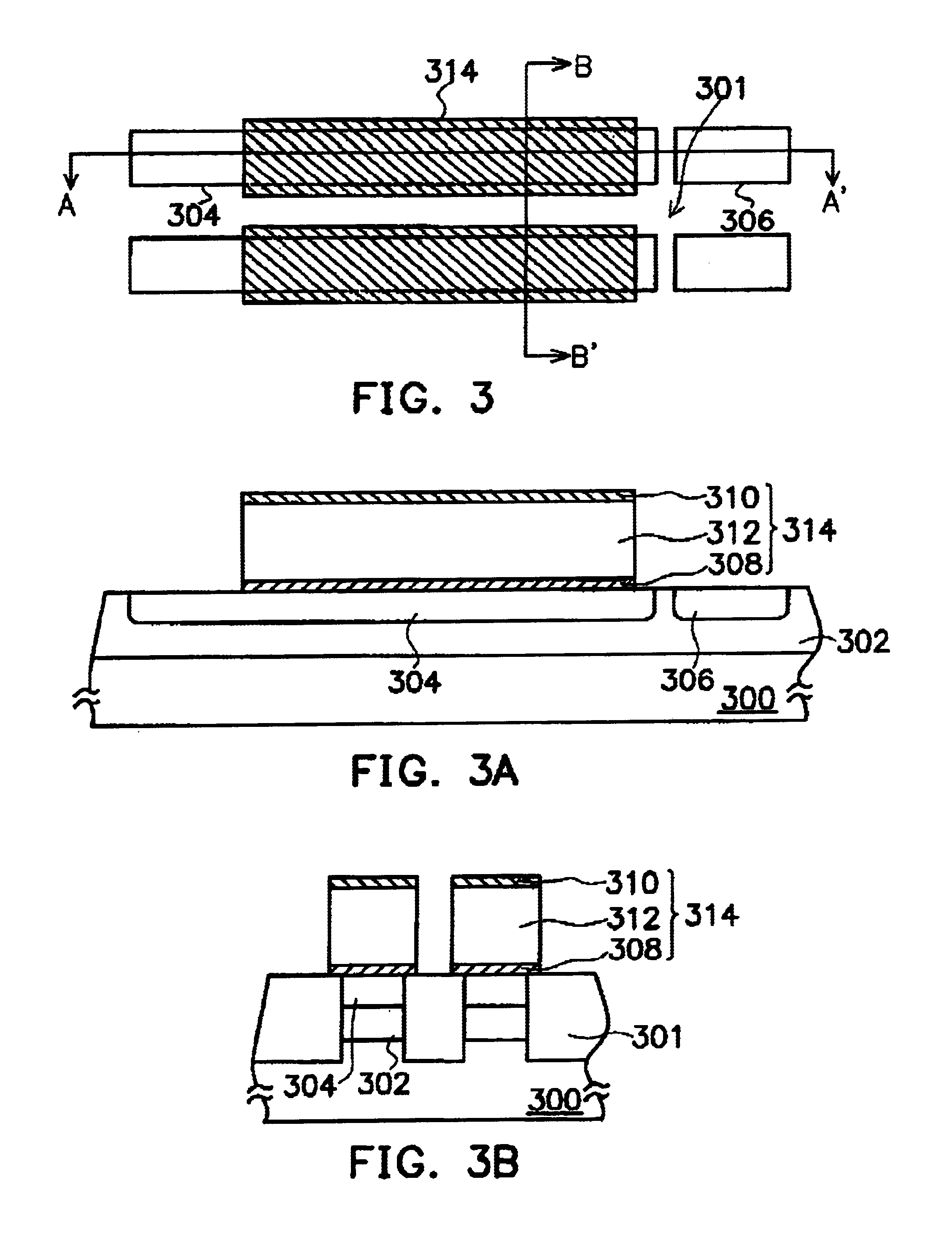
[0029]FIGS. 3-6 are top views of the process of fabricating a resistance random access memory in accordance with a preferred embodiment of the present invention. FIGS. 3A-6A are cross-sections (along A-A′) of the process of fabricating a resistance random access memory in accordance with a preferred embodiment of the present invention.

[0030]FIGS. 3B-6B are cross-sections (along B-B′) of the process of fabricating a resistance random access memory in accordance with a preferred embodiment of the present invention.

[0031]Referring to FIGS. 3, 3A, and 3B, a substrate 300 such as N-type substrate is provided. Then isolated regions 301 are formed in substrate 300. P-type doped regions 302 then are formed between the isolated regions 301 as word lines. The N+ doped region 304 and a P+ doped region 306 are formed in word line 302. The N+ doped region 304 and the P+ doped region 306 constitutes a diode. The N+ doped region 304 is also used as a reset line. The P+ doped region 306 provides th...


PUM


Abstract

The present invention provides a resistance random access memory structure, including a plurality of word lines in a substrate, a plurality of reset lines coupled to the word lines, a dielectric layer on the substrate, a plurality of memory units in the dielectric layer. Each of the memory units includes a bottom electrode, a top electrode and a resistive thin film between the top electrode and the bottom electrode. The top electrodes of the memory units in a same column e coupled to one of the reset lines and a plurality of the bit lines on the memory units. The bottom electrodes of the memory units in a same row are coupled to one of the bit lines. Because the present invention provides reset lines for Type 1R1D RRAM, it can overcome the non-erasable of the conventional Type 1R1D RRAM.

Description

CROSS REFERENCE TO RELATED APPLICATIONS[0001]This application claims the priority benefit of Taiwan application serial no. 92115025, filed Jun. 3, 2003.BACKGROUND OF INVENTION[0002]1. Field of the Invention[0003]This invention generally relates to a semiconductor device and method for fabricating the same, and more particularly to a resistance random access memory (“RRAM”) device and method for fabricating the same.[0004]2. Description of the Related Art[0005]Colossal magneto resistive (“CMR”) thin films and oxidation thin films having Perovskite structure are resistance-reversible materials which can be applied to reversible switching process. For colossal magneto resistive thin film, when a positive impulse (voltage) is applied to it, its resistance is programmed to high resistance; when a negative impulse (voltage) is applied, its resistance is programmed to low resistance. For the oxidation thin film having Perovskite structure, when a positive impulse (current) is applied to it...

Claims


Application Information

Patent Timeline
Patent Type & Authority Patents(United States)
IPC IPC(8): G11C13/00H01L27/10H01L27/24
CPCG11C13/0007H01L27/24H01L27/101G11C2213/31H10B63/20H10B63/80H10B63/00
Inventor JANG, WEN-YUEH
Owner WINBOND ELECTRONICS CORP
Why Eureka
Try Eureka