Conformable layered antenna array

a technology of layered antenna arrays and antenna arrays, which is applied in the field of antenna arrays, can solve the problems of high cost of manufacturing structures, large physical size and relatively heavy weight, and the need to improve the manufacturing process and the resulting mechanical structure, and achieve the effect of low cos

Inactive Publication Date: 2005-09-20
COMMSCOPE TECH LLC
View PDF24 Cites 34 Cited by
  • Summary
  • Abstract
  • Description
  • Claims
  • Application Information

AI Technical Summary

Benefits of technology

[0010]The antenna array in accordance with an embodiment of the invention is formed of a plurality of layers, the layers preferably bonded to one another. The array may include a plurality of metallic radiator elements formed on two or more dielectric layers, which are in turn bonded onto a metallic ground layer. The thicknesses of the dielectric layers are chosen to provide the desired spacing for the operation of the radiator elements. The radiator elements may be preferably formed on a flexible dielectric carrier layer and the carrier layer may be bonded to a dielectric foam core layer that can be flexible or can be molded or cut to planar or non-planar shapes. The array may include one or more dielectric layers with a plurality of parasitic radiator elements formed thereon, where the dielectric layers preferably are bonded on top of the metallic radiator elements. The layers and ground can be enclosed in a structure that includes a radome and provides for environmental protection and facilitates mounting the antenna assembly in a secure and robust manner to other structures.
[0012]The low-cost antenna array design in accordance with embodiments of the invention uses low-cost individual components suitable for printed circuit board manufacturing techniques that can be assembled in a short period of time with little or no required adjustment to achieve the desired performance after assembly.

Problems solved by technology

These antenna arrays generally have a large number of components, a high cost for manufacturing the structures, large physical size and a relatively heavy weight.
The individual metal parts are typically stamped from aluminum sheet stock and then assembled in a labor-intensive operation.
High performance PTFE based PCB materials have a significantly higher cost compared to other types of PCB materials.
While these conventional array structures have improved some characteristics of antenna arrays, such as the number of components and weight, the electrical performance, the cost of the manufacturing process and the resulting mechanical structures need to be improved.

Method used


Image

  • Conformable layered antenna array
  • Conformable layered antenna array
  • Conformable layered antenna array

Examples


embodiment 110

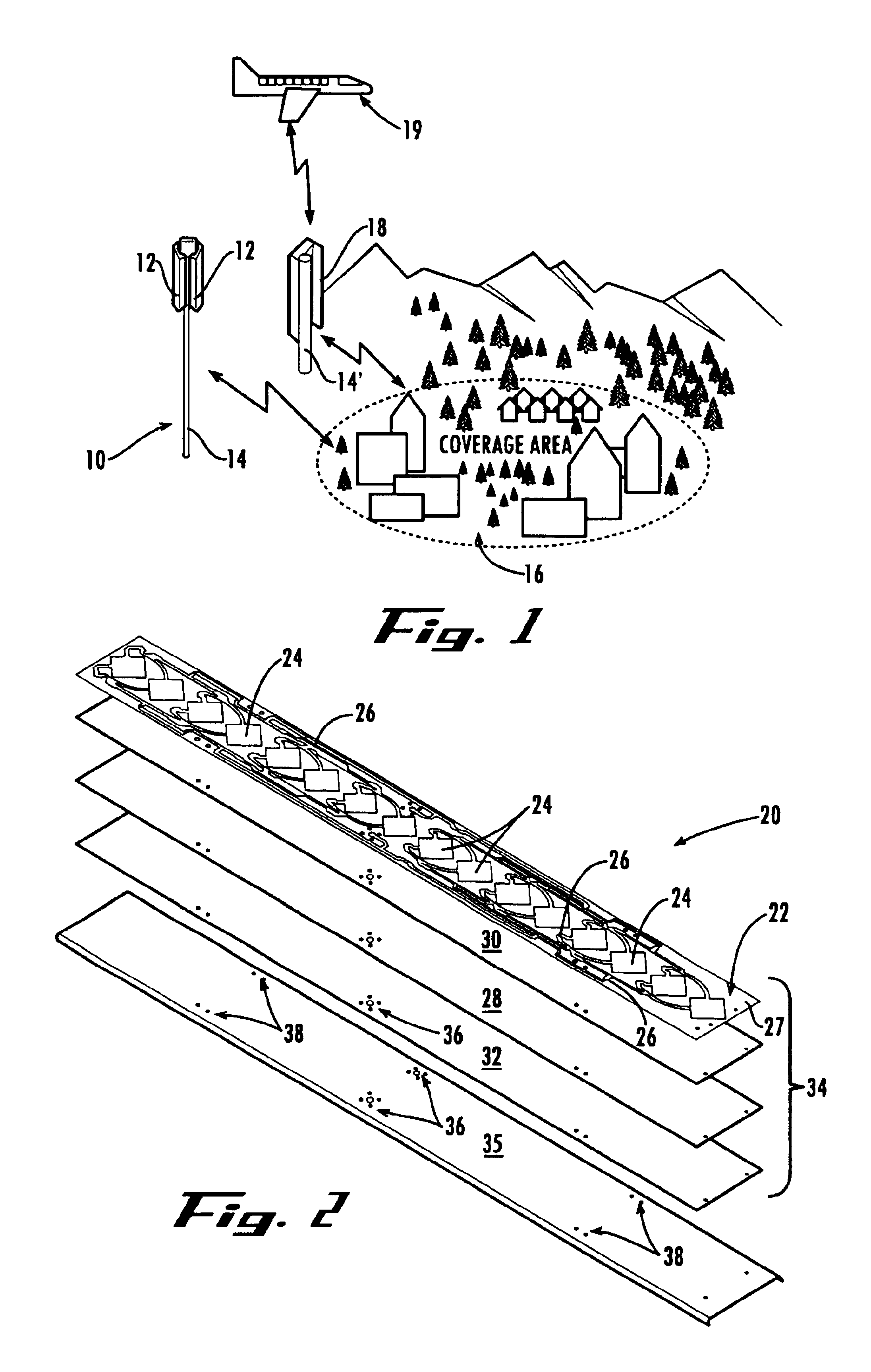
[0071]FIG. 20 is a diagrammatic illustration of the utilization of a pair of curved antenna arrays 110 of the present invention in a base-station environment. FIG. 20 illustrates two arrays 110 that have a subsection 112 of each array that is non-planar. The embodiment 110 provides for coverage that emphasizes the regions to the sides of the mounting structure while providing for a portion of the energy to be directed above the mounting structure. This can be particularly important in providing shaped beam coverage as is often desired for communications with aircraft from the ground where the need for the greatest antenna directivity is near the horizon and there is a need to provide continuous coverage to zenith relative to the mounting structure. The arrays 110 can be mounted on the top of the cell tower 14′ and include an arcuate upper end 112 to provide coverage to objects or elevations above the cell tower 14′ as illustrated by the curved antennas 18 in FIG. 1.

first embodiment

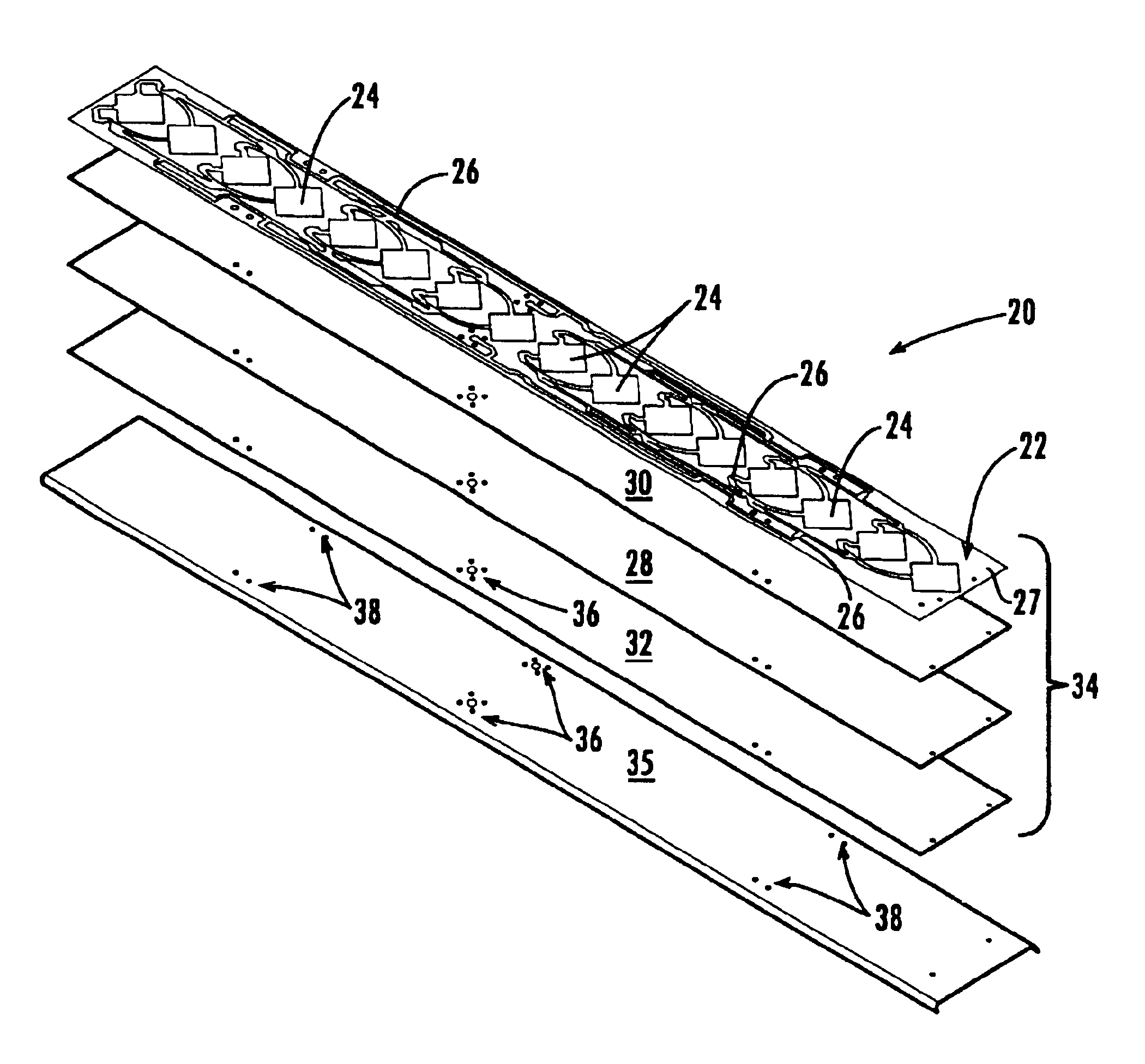
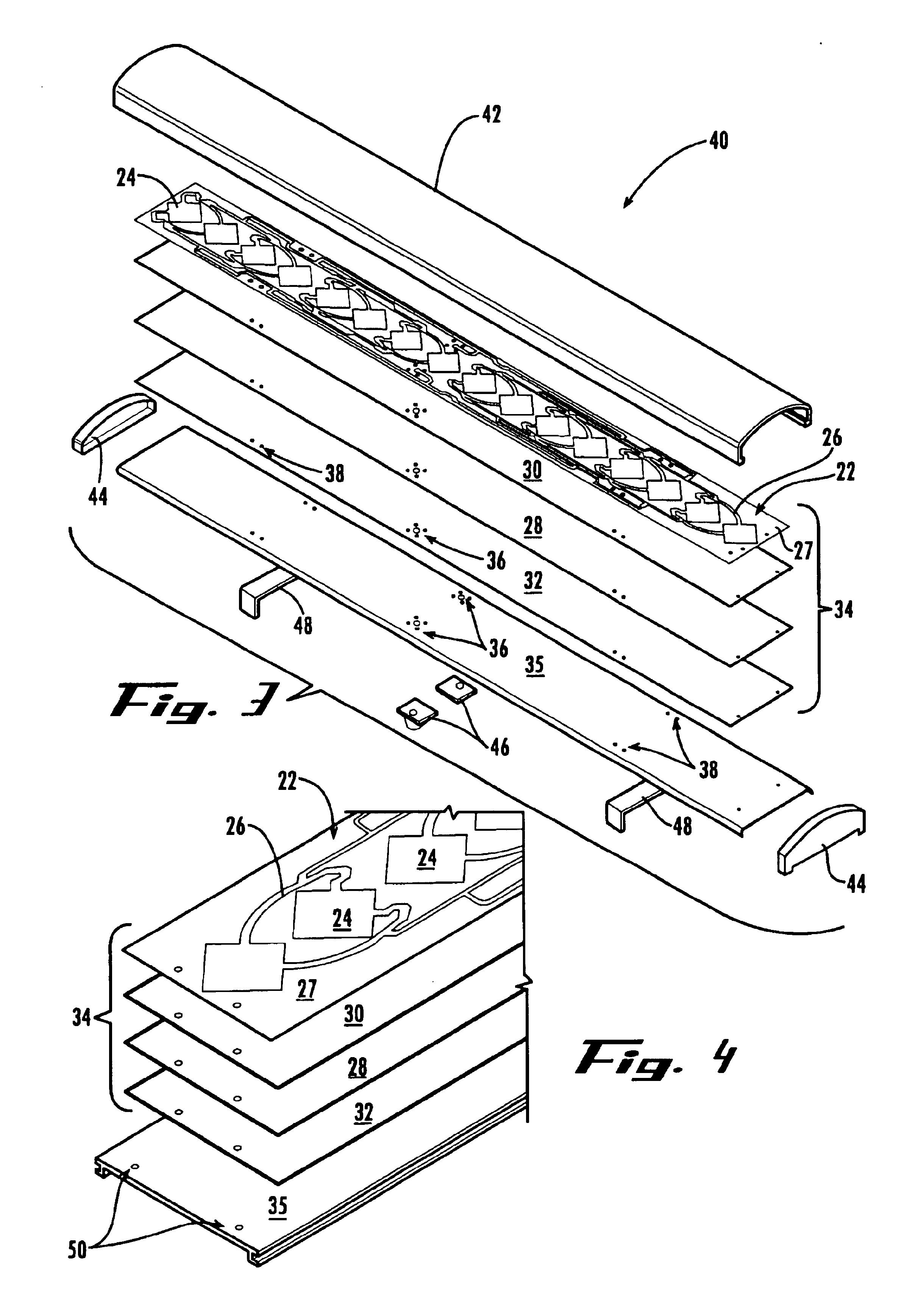
[0072]Referring now to FIG. 21, a method 120 for manufacturing the antenna arrays of the present invention is illustrated. Referring to FIG. 5, embodiments of manufacturing the antenna 20 will first be described. The metallic layer 60 is first bonded to the carrier dielectric layer 27 utilizing the adhesive layer 62 in a step 122. The carrier dielectric layer 27 then is bonded to the foam core dielectric layer 28 utilizing the adhesive layer 30 in a step 124. The dielectric layer 27 generally is a thin carrier layer for the layer 60, while the layer 28 provides the desired dielectric distance or thickness for the proper operation of the radiators 24.

[0073]The adhesive layer 32 then can be bonded to the dielectric layer 28 to form the stack or sandwich 34 in a step 126. The adhesive layer 32 preferably is a double-sided dielectric tape with a release layer (not illustrated) opposite the layer 28. The antenna electrical elements, the radiators 24 and the circuitry 26, then preferably ...


PUM


Abstract

A low-cost antenna array and method of manufacturing the array, in a planar form or in a structurally flexible or curved array structure are shown. The antenna array has a plurality of metallic antenna electrical and radiator elements formed on a foam core layer bonded onto a metallic ground layer. The radiator elements preferably are formed on a thin dielectric carrier layer bonded to the foam core layer. The array can include one or more additional dielectric layers, each with a plurality of parasitic radiator elements formed thereon, mounted on top of the electrical elements. Manufacturing the array preferably includes bonding the layers to one another. The electrical and radiator elements are formed, preferably by etching, before the foam core layer is bonded to the ground layer. The additional dielectric layer and the parasitic radiators then are bonded to the already formed electrical elements on the ground layer.

Description

BACKGROUND OF THE INVENTION[0001]1. Field of the Invention[0002]The present invention relates to antenna arrays and, more particularly, is directed to low-cost antenna arrays and methods of manufacturing antenna arrays having substantially planar and curved surfaces for telecommunications applications.[0003]2. Description of the Related Art[0004]Antenna arrays have been manufactured in a variety of forms and have many different applications in the communications field. One particular application with a high volume and an emphasis on cost of the antenna arrays is for use in base-stations of mobile communication systems, such as cellular transmissions operating at about 800 MHz and Personal Communication Services (PCS) transmissions operating at about 1900 MHz in the United States, as well as other wireless and mobile communication applications worldwide.[0005]Base-station antenna arrays have been formed using a wide variety of structures having significant variations in size, cost an...

Claims


Application Information

Patent Timeline
Patent Type & Authority Patents(United States)
IPC IPC(8): H01Q9/04H01Q1/08H01Q1/24H01Q21/08
CPCH01Q1/085H01Q1/246H01Q9/0414H01Q21/08
Inventor TILLERY, JAMESRUNYON, DONALD L.
Owner COMMSCOPE TECH LLC
Why Eureka
Try Eureka