Microminiature image pickup device

a micro-miniature and image technology, applied in the field of image pickup devices, can solve the problems of long processing time and manual operation

Inactive Publication Date: 2005-09-20
TEXAS INSTR INC
View PDF6 Cites 52 Cited by
  • Summary
  • Abstract
  • Description
  • Claims
  • Application Information

AI Technical Summary

Benefits of technology

[0025]If the microminiature image pickup device is constituted in this way, it will be possible for the first electronic component and the second electronic component to be disposed in positions where they are stacked in the diametral direction perpendicular to the lengthwise orientation of the microminiature image pickup device, so that the microminiature image pickup device can be shortened in the length direction.
[0027]In addition, the electrical connection between the electrode of the image pickup device, e.g., CCD, and the stacked circuit board is accomplished with a connection member, e.g., TAB tape, and a soldered lead as used in the past is not required. Thus processing will be simple and the assembly processing time can also be reduced.

Problems solved by technology

The problem has been that a manual operation is required, and on top of that, the processing time is long.

Method used


Image

  • Microminiature image pickup device
  • Microminiature image pickup device

Examples


embodiment 1

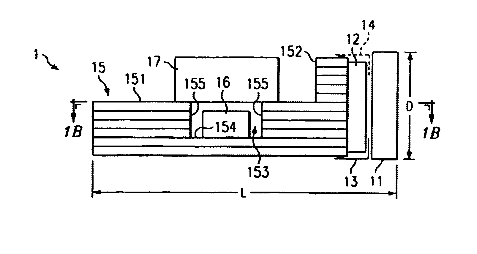
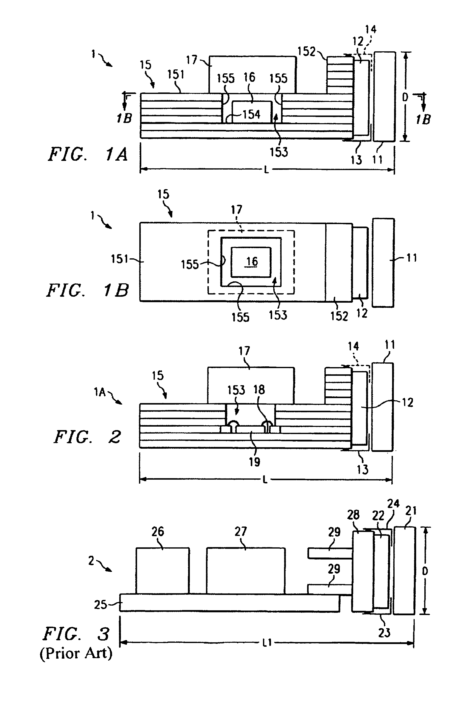
[0056]A microminiature CCD image pickup device that is a first embodiment of this invention will be discussed, with reference to FIGS. 1(A) and (B).

[0057]FIG. 1(A) is a side view of microminiature CCD image pickup device (1) and FIG. 1(B) is a top view.

[0058]Microminiature CCD image pickup device (1) has optical glass (11), CCD chip (12), and stacked circuit board (15) disposed along its length direction.

[0059]The inner surface of optical glass (11) and one surface of CCD chip (12) touch, and the other surface of CCD chip (12) touches the side surface of stacked circuit board (15).

[0060]TAB (Tape Automated Bonding) tape (13), which is known in semiconductor device packaging technology, is connected to the electrode of CCD chip (12) and the wiring pattern of stacked circuit board (15). Drive power is supplied from the outside to CCD chip (12), enabling CCD chip (12) to operate. The signals comprising the image pickup output from CCD chip (12) are transmitted to stacked circuit board ...

embodiment 2

[0085]A microminiature CCD image pickup device that is a second embodiment of this invention will be discussed with reference to FIG. 2.

[0086]FIG. 2 is a cross section of microminiature CCD image pickup device (1A) that is a second embodiment of this invention.

[0087]Microminiature CCD image pickup device (1A) shown in FIG. 2 has optical glass (11), CCD chip (12), and stacked circuit board (15) disposed along its length direction. The constitution of these is the same as in the first embodiment.

[0088]Stacked circuit board (15) also has the same constitution as the first embodiment.

[0089]The electrical connection of CCD chip (12) and stacked circuit board (15) is also accomplished with TAB tape (13), in the same way as in the first embodiment.

[0090]In the second embodiment, the difference is that miniature chip component (16) in FIG. 1 is assembled on electrical connection surface (18) in cavity (153) as bare chip (19) that is well known as a semiconductor packaging technology. The sp...


PUM


Abstract

A microminiature CCD image pickup device with a shortened length that can be applied to an electronic medical endoscope or the like. Microminiature CCD image pickup device (1) has optical glass (11), CCD chip (12), and stacked circuit board (15) that are disposed in that order along its length orientation. It further has TAB tape (13) that connects CCD chip (12) and the electronic circuits mounted on stacked circuit board (15). Stacked circuit board (15) is formed with insulated circuit board in which are packaged electronic circuits, including their wiring pattern, stacked in stacked layers in the diametral direction perpendicular to said length orientation, and has at least one cavity (153) formed as an indention in the diametral direction. At least one miniature chip component (16) is mounted in cavity (153), and at least one chip component (17) is mounted on the surface of stacked circuit board (15) over cavity (153). The electronic circuits are stacked in stacked circuit board (15) and chip components (16) and (17) are disposed in the diametral direction, so that the length of microminiature CCD image pickup device (1) is shortened.

Description

FIELD OF THE INVENTION[0001]This invention pertains to an image pickup device that uses a charge coupled device (CCD), such as is used for the tip of an electronic medical endoscope, for example. Specifically, it pertains to a microminiature image pickup device in which the dimension in the length direction is shortened.BACKGROUND OF THE INVENTION[0002]An example of a microminiature CCD image pickup device used as an ultrasmall image pickup device for an electronic medical endoscope is shown.[0003]Microminiature CCD image pickup devices used for electronic medical endoscopes have been made as small as possible in order to reduce pain to which the patient is subjected from swallowing the microminiature CCD image pickup device when a patient's stomach is to be examined, for example.[0004]To try such miniaturization, the external dimensions of the tip part of the microminiature CCD image pickup device may be miniaturized and the length of the microminiature CCD image pickup device may ...

Claims


Application Information

Patent Timeline
Patent Type & Authority Patents(United States)
IPC IPC(8): A61B1/04H01L27/148H01L27/14H01L31/02H05K3/46H04N5/225H04N7/18H05K1/18H04N5/335H04N5/372
CPCH04N5/2251H04N5/2253H04N2005/2255H05K1/183H05K3/4611H01L2224/48091H01L2224/48227H01L2924/00014H04N23/555H04N23/54
Inventor KOMORO, ATSUSHIYAMASHITA, TOMOKAZU
Owner TEXAS INSTR INC
Why Eureka
Try Eureka