CPP mode magnetic sensing element including a multilayer free layer biased by an antiferromagnetic layer

a free layer, antiferromagnetic layer technology, applied in the field of current perpendicular to the plane (cpp) magnetic sensing elements, can solve the problems of degrading read sensitivity , not being able to fabricate a magnetic sensing element with excellent read sensitivity, and not being able to improve read sensitivity and read output simultaneously, so as to improve the structure of the free magnetic layer and improve the read sensitivity . , the effect of improving the read

Inactive Publication Date: 2005-09-20
TDK CORPARATION
View PDF14 Cites 17 Cited by
  • Summary
  • Abstract
  • Description
  • Claims
  • Application Information

AI Technical Summary

Benefits of technology

[0025]It is an object of the present invention to provide a magnetic sensing element in which both read sensitivity η and read output are improved by the improved structure of the free magnetic layer, and which is thereby suitable for miniaturization of the element.

Problems solved by technology

However, if the thickness h1 of the free magnetic layer 8 is increased, the demagnetizing field of the free magnetic layer 8 is increased, resulting in a degradation in the read sensitivity η.
As a result, it is not possible to fabricate a magnetic sensing element with excellent read sensitivity.
That is, in any case, in the conventional CPP magnetic sensing element having a structure including the means for applying the longitudinal bias magnetic field shown in FIG. 7, it is not possible to improve read sensitivity η and read output simultaneously.

Method used


Image

  • CPP mode magnetic sensing element including a multilayer free layer biased by an antiferromagnetic layer
  • CPP mode magnetic sensing element including a multilayer free layer biased by an antiferromagnetic layer
  • CPP mode magnetic sensing element including a multilayer free layer biased by an antiferromagnetic layer

Examples


first embodiment

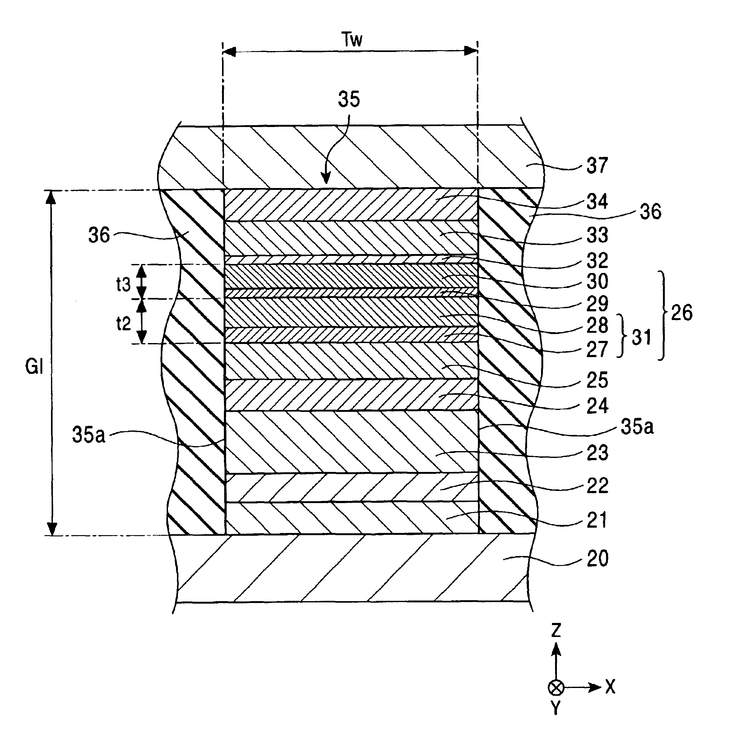
[0049]FIG. 1 is a partial sectional view which shows an overall structure of a magnetic sensing element in the present invention, viewed from the surface facing a recording medium. In FIG. 1, only the central part of the element is shown.

[0050]The magnetic sensing element shown in FIG. 1 reads the signals written in the recording medium. Although not shown in the drawing, an inductive head for writing may be deposited on the magnetic sensing element.

[0051]The magnetic sensing element is formed on the trailing end of a slider, for example, composed of alumina-titanium carbide (Al2O3-TiC). The slider is connected to an elastically deformable support composed of a stainless steel or the like at a surface opposite to the surface facing the recording medium, and thus a magnetic head device is produced.

[0052]A lower shielding layer 20 is composed of a magnetic material, such as a NiFe alloy, and also acts as a lower electrode in this embodiment.

[0053]An underlayer 21 composed of a nonmagn...

second embodiment

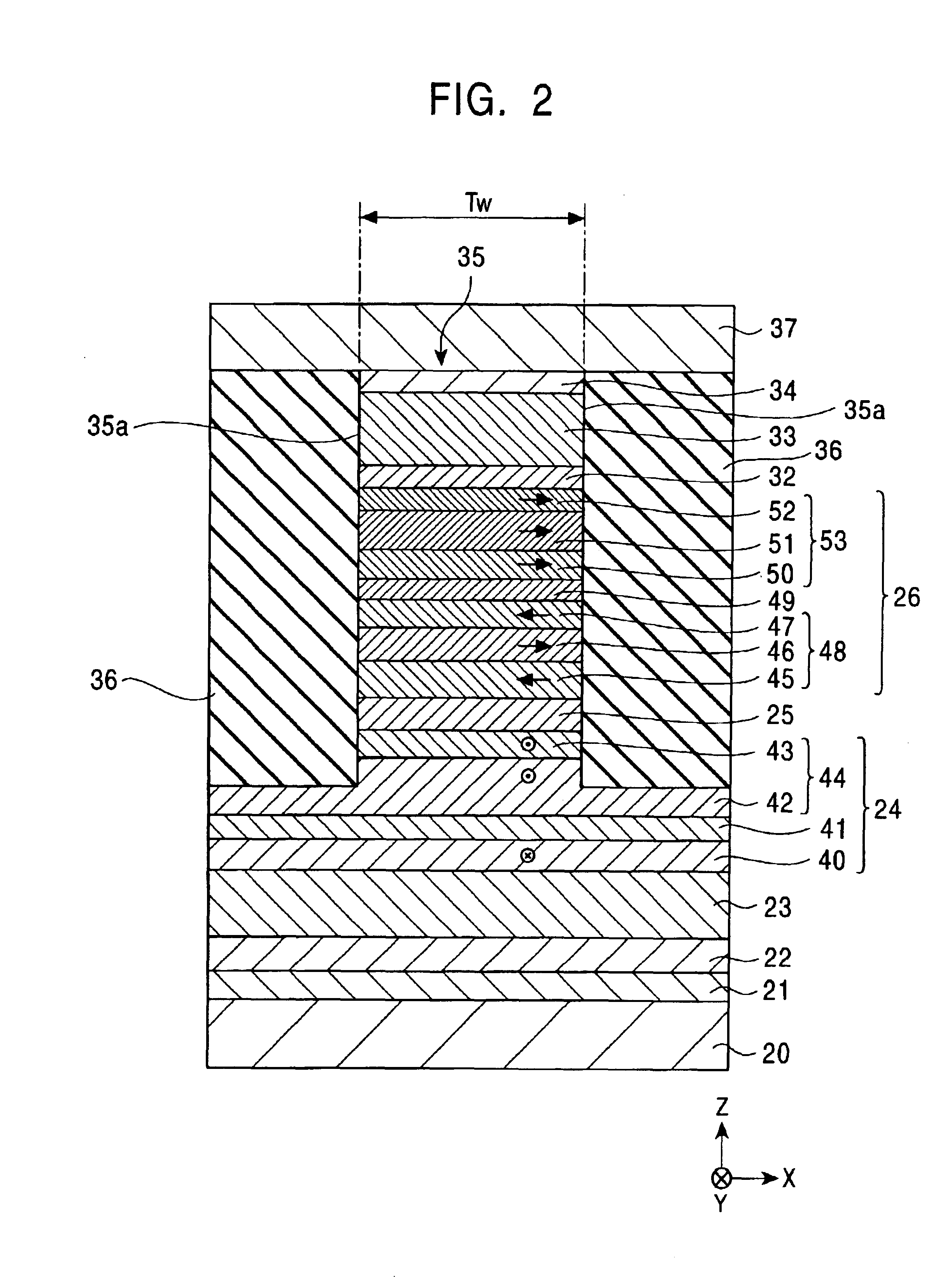
[0102]FIG. 2 is a partial sectional view of a magnetic sensing element in the present invention, viewed from the surface facing a recording medium. The same reference numerals as those in FIG. 1 are used in FIG. 2 for the same layers.

[0103]In the embodiment shown in FIG. 2, a free magnetic layer 26 also has a laminated ferrimagnetic structure, and a second nonmagnetic layer 32 and a second antiferromagnetic layer 33 are deposited on a surface of a first free magnetic sublayer 53 opposite to the surface in contact with a nonmagnetic intermediate sublayer 49.

[0104]Consequently, unidirectional interlayer exchange coupling is produced between the first free magnetic sublayer 53 and the second antiferromagnetic layer 33, and the first free magnetic sublayer 53 is aligned in a single domain state in the track width direction. The free magnetic layer 26 has the laminated ferrimagnetic structure and the physical thickness of the free magnetic layer 26 corresponds to the total thickness of t...

third embodiment

[0123]FIG. 3 is a partial sectional view of a magnetic sensing element in the present invention, viewed from the surface facing a recording medium.

[0124]In the embodiment shown in FIG. 3, the magnetic sensing element has the same structure as that of the magnetic sensing element shown in FIG. 2 except that layers between the underlayer 21 and the protective layer 34 in the multilayer film 35 shown in FIG. 2 are deposited in the reversed order.

[0125]That is, in the embodiment shown in FIG. 3, an second antiferromagnetic layer 33, a second nonmagnetic layer 32, a first free magnetic sublayer 53, a nonmagnetic intermediate sublayer 49, a second free magnetic sublayer 48, a first nonmagnetic layer 25, a second pinned magnetic sublayer 44, a nonmagnetic intermediate sublayer 41, a first pinned magnetic sublayer 40, and a first antiferromagnetic layer 23 are deposited in that order above an underlayer 21. The materials and thicknesses for the individual layers are the same as those descri...


PUM

PropertyMeasurementUnit
width Twaaaaaaaaaa
antiferromagneticaaaaaaaaaa
nonmagneticaaaaaaaaaa

Abstract

In a CPP magnetic sensing element, a free magnetic layer has a laminated ferrimagnetic structure. Since the physical thickness of the free magnetic layer is increased, the product of a change in resistance ΔR and an area A can be improved and read output can be improved. Since the magnetic thickness is decreased, the demagnetizing field of the free magnetic layer is weakened, and it is possible to stably apply a continuous bias with a proper magnitude from the second of two antiferromagnetic layers to the first free magnetic sublayer. Therefore, it is possible to fabricate a magnetic sensing element with satisfactory read sensitivity η.

Description

[0001]This application claims the benefit of priority to Japanese Patent Application 2002-114296, filed on Apr. 17, 2002.BACKGROUND OF THE INVENTION[0002]1. Field of the Invention[0003]The present invention relates to current-perpendicular-to-the-plane (CPP) magnetic sensing elements and, more particularly, to a magnetic sensing element in which read sensitivity and read output can be improved even when the track is narrowed.[0004]2. Description of the Related Art[0005]FIG. 7 is a partial sectional view of a conventional CIP magnetic sensing element, viewed from the surface facing a recording medium. Herein, CIP stands for current-in-the-plane, and in the CIP magnetic sensing element, a sensing current flows parallel to the planes of a multilayer film which is located in the center of the magnetic sensing element.[0006]Referring to FIG. 7, the magnetic sensing element includes a lower shielding layer 1 composed of Permalloy (NiFe alloy) or the like and a lower gap layer 2 composed o...

Claims


Application Information

Patent Timeline
Patent Type & Authority Patents(United States)
IPC IPC(8): G01R33/06G01R33/09G11B5/39H01F10/16H01F10/32H01L43/08
CPCB82Y10/00B82Y25/00G01R33/093G11B5/3903G11B5/3909G11B2005/3996
Inventor SAITO, MASAMICHI
Owner TDK CORPARATION
Why Eureka
Try Eureka