Two-dimensional structural transition controlled by an electric field, memory storage device thereof, and method of making a memory storage device

a two-dimensional structural transition and electric field technology, applied in information storage, instruments, nanotechnology, etc., can solve the problem of often induced mechanism of structure change, and achieve the effect of broad applicability

Inactive Publication Date: 2005-09-20
UNIVERSITY OF BASEL
View PDF11 Cites 13 Cited by
  • Summary
  • Abstract
  • Description
  • Claims
  • Application Information

AI Technical Summary

Benefits of technology

[0026]The molecules used in the present invention can be synthesized using existing methods. The immobilization of these molecules at the substrate surface enables the use of micro- and nano-fabrication tools and methods for optional further processing. The disclosed molecule, structured medium, and methods enable a broad applicability, and a variety of combinations with other established and exploratory methods. The large variety of molecules that fall into the class of the disclosed molecules as well as the large variety of the disclosed substrates enables broad range of applications and combinations with other established and exploratory techniques.

Problems solved by technology

The dramatic progress of the computer technology over the last four decades has been fueled by an unparalleled development of the basic hardware elements: storage devices, processors and displays.
However, usually bulk material is used to achieve these methods and the mechanism of changing the structure is often induced by resistive heat.
However, the prior art liquid crystal devices have the following drawbacks.
First, they require a three-dimensional structural transition that is a relatively bulky, multilayer structure that is about 50-100 μm thick.

Method used


Image

  • Two-dimensional structural transition controlled by an electric field, memory storage device thereof, and method of making a memory storage device
  • Two-dimensional structural transition controlled by an electric field, memory storage device thereof, and method of making a memory storage device
  • Two-dimensional structural transition controlled by an electric field, memory storage device thereof, and method of making a memory storage device

Examples


Embodiment Construction

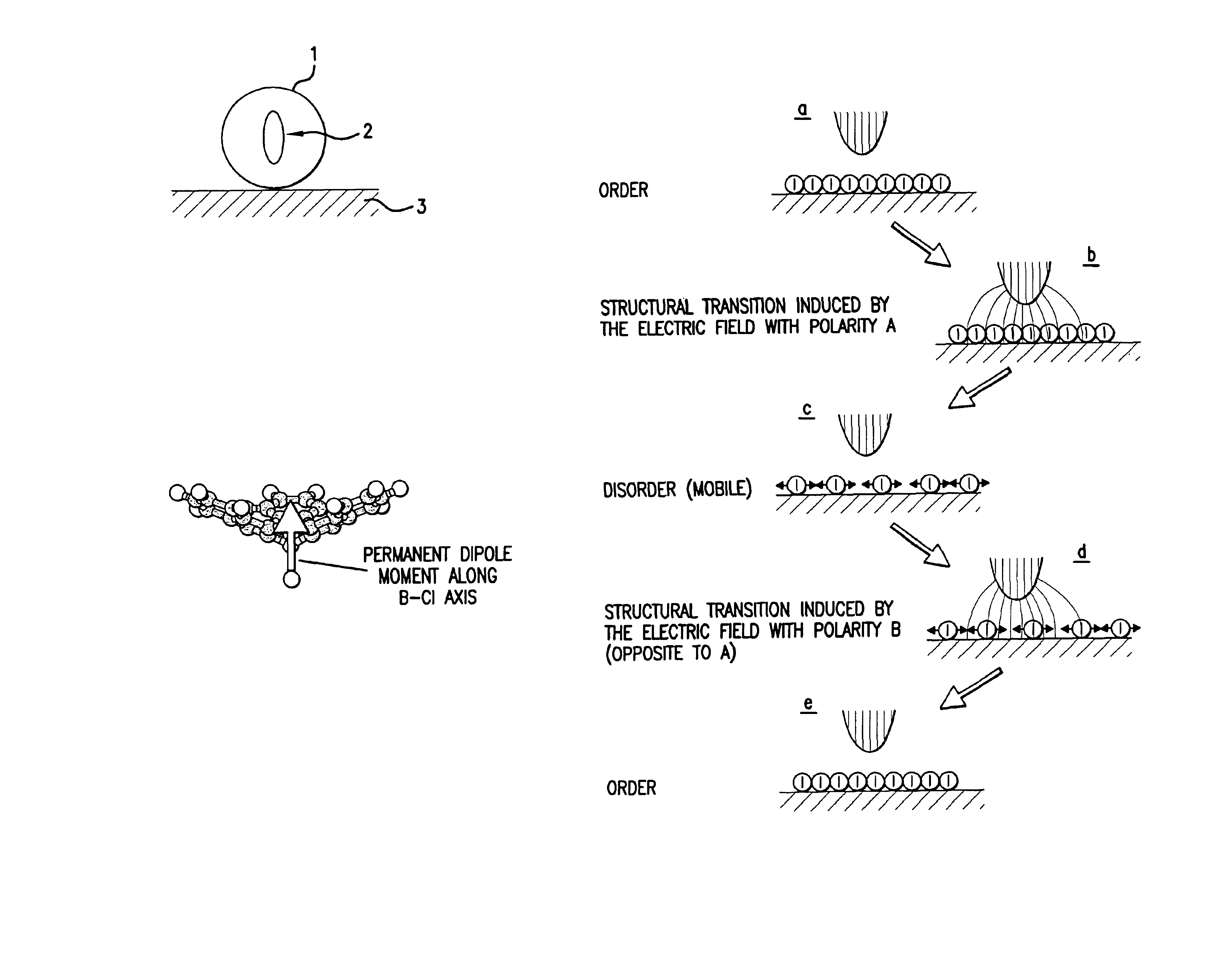
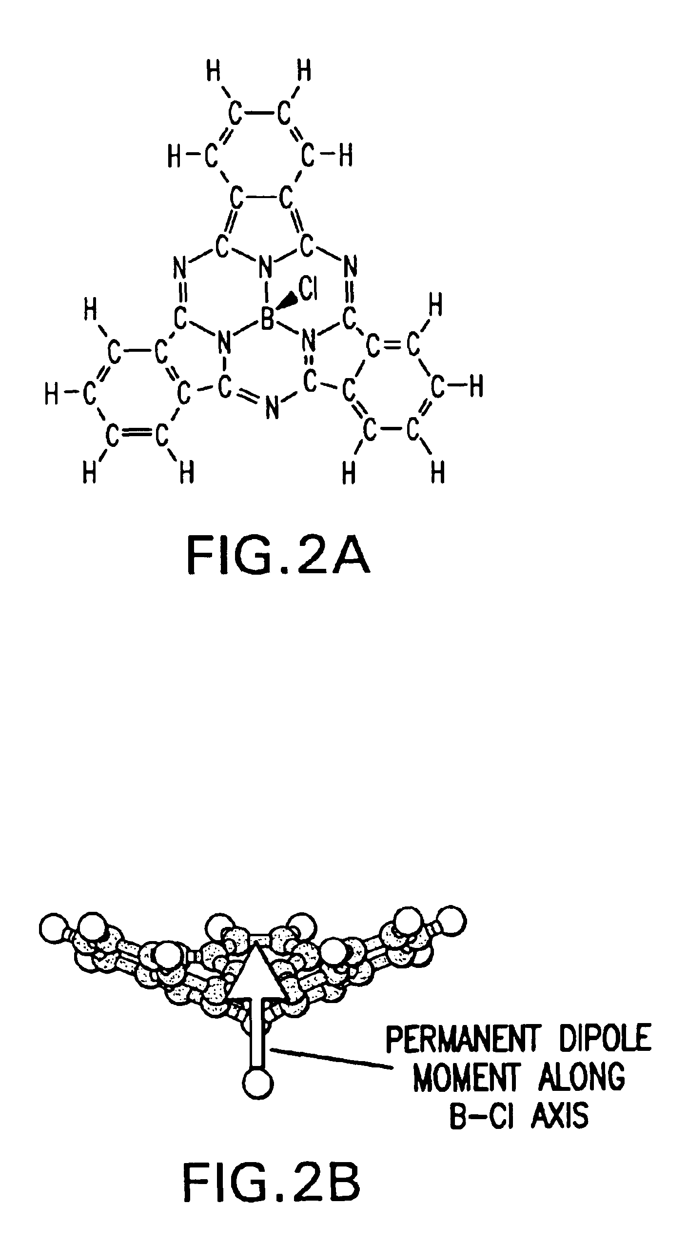
[0050]The present invention utilizes a mono-layer, or sub-monolayer, of molecules that have a permanent dipole moment with a reversible structural transition property so as to provide novel high density memory devices, locally switchable mirror surfaces, locally switchable surface lubricants, lithographic applications for patterning molecular layers, and lithographic applications for substrate patterning. Thus, the present invention can also be used for the controlled change of local surface properties in a variety of different applications. Memory devices manufactured using a dipole layer in accordance with the present invention are electrically addressable thereby permitting effective reading and writing, and provide a high memory density (e.g. 1012 bits / inch2).

[0051]To facilitate an easy understanding of the present invention, certain terms used are defined below. Then, a class of molecules having permanent dipole moments and which show a reversible transition between different s...


PUM

PropertyMeasurementUnit
diameteraaaaaaaaaa
viscosityaaaaaaaaaa
thickaaaaaaaaaa

Abstract

This invention relates to the controlled two-dimensional structural transition of a dipole monolayer at a metal, semi-conducting or insulating interface. The dipole monolayer consists of objects / molecules with a permanent electric dipole moment. A transition between the structures of the molecular layer can be performed locally and reversibly by applying an electrical field and the structures / patterns can be reversibly switched many times between two different structures / states. Both of the two structures, the ordered and the disordered structures, are intrinsically stable without the presence of the switching electrical field. This controlled switch of the local layer structure can be used to change layer properties (i.e., mechanical, electrical, optical properties). The controlled reversible modifications of the dipole monolayer structures are usable as bit assignments in data storage applications for example.

Description

[0001]The present application for patent claims priority under 35 U.S.C. § 119(e) to U.S. Provisional Application No. 60 / 477,062, filed on Jun. 10, 2003, and which is incorporated herein by reference in its entirety.FIELD OF THE INVENTION[0002]The present invention relates to a molecular dipole layer that has the property of ordering into different structures on a metallic, semi-conducting or insulating substrate. Also, in accordance with the present invention, a method of reversibly changing the structure of the molecular dipole layer into the different structures by applying a selectively polarized electric field is described. Both the molecular dipole layer and the method of reversibly switching between various structures using a selectively polarized electric field can be applied to a variety of usages such as the manufacture of patterned layers with specific electrical, optical and mechanical properties for lithography, data storage and display technology (i.e., switching mirro...

Claims


Application Information

Patent Timeline
Patent Type & Authority Patents(United States)
IPC IPC(8): G11C13/02
CPCB82Y10/00G11C13/0014G11C13/02Y10S977/943
Inventor BERNER, SIMONSCHINTKE, SILVIARAMOINO, LUCADE WILD, MICHAELJUNG, THOMAS A.
Owner UNIVERSITY OF BASEL
Why Eureka
Try Eureka