Using data compression for faster testing of embedded memory

a technology of embedded memory and data compression, which is applied in the field of embedded memory testing, can solve the problems of increasing the number of pins on the chip that are available for external testing, the major problem of pin limitation, and the increasing cost driving factor of the total chip cost of the chip

Inactive Publication Date: 2005-09-27
INFINEON TECH AG
View PDF7 Cites 23 Cited by
  • Summary
  • Abstract
  • Description
  • Claims
  • Application Information

AI Technical Summary

Problems solved by technology

One limitation is the maximum clock frequency that an external tester can apply to the chip, and the other limitation is the number of pins on the chip that are available for use by the external tester.
When testing an embedded memory such as an embedded DRAM, the aforementioned pin limitation is the major...

Method used


Image

  • Using data compression for faster testing of embedded memory
  • Using data compression for faster testing of embedded memory
  • Using data compression for faster testing of embedded memory

Examples


Embodiment Construction

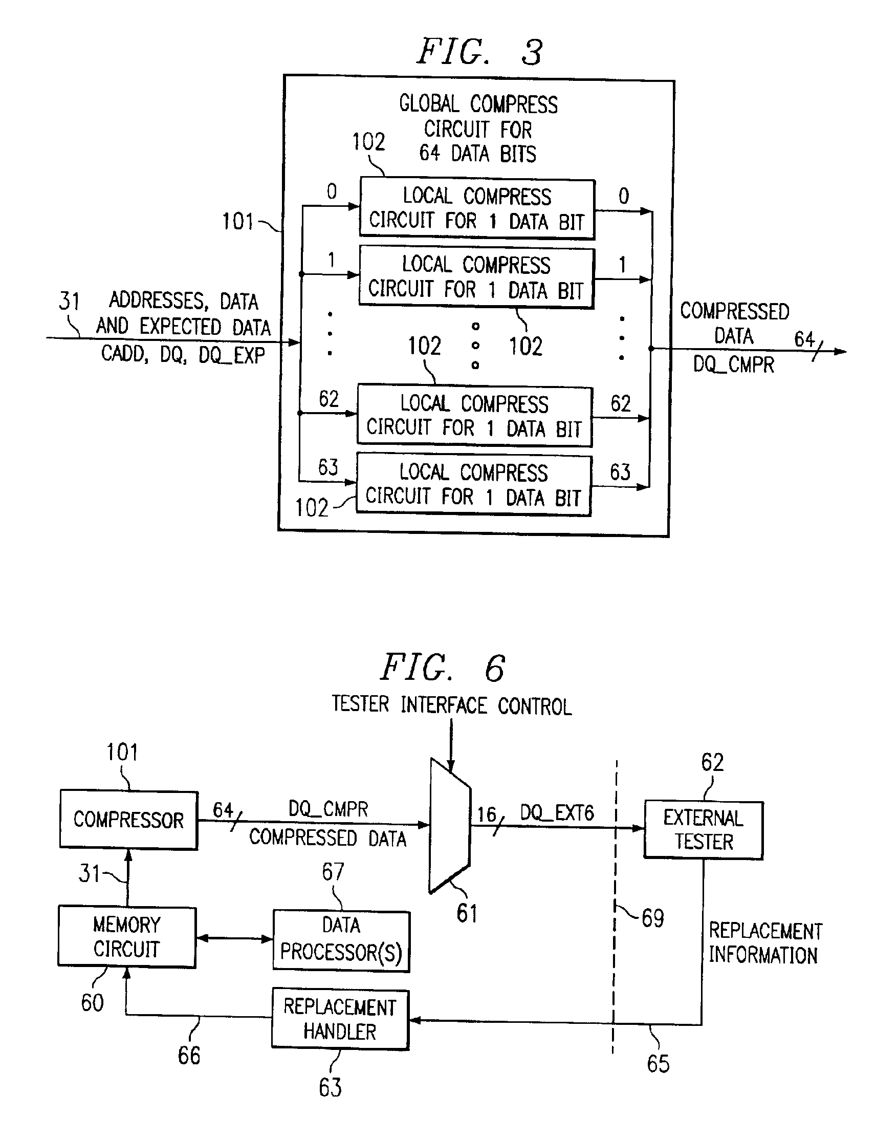
[0016]FIG. 3 diagrammatically illustrates exemplary embodiments of a global compression circuit 101 for use in embedded memory testing according to the invention. In the exemplary embodiments of FIG. 3, the global compression circuit 101 is coupled to an address bus and a data bus of a memory circuit, thereby to receive address information used by the memory circuit and data stored in the memory circuit. The global compression circuit 101 is also connected to receive expected data, which will be compared to the data received from the memory data bus. The aforementioned address, data and expected data information received by the global compression circuit 101 is indicated generally at 31 in FIG. 3.

[0017]In some embodiments, the memory data bus is 64 bits wide, so the circuit 101 can receive 64 data bits from the memory data bus. These 64 data bits can, for example, correspond to a 64-row×1 column portion of a memory array (for example a DRAM array) implemented by the memory circuit. ...


PUM


Abstract

A memory apparatus is configured by obtaining test information for each of group of memory locations within the memory apparatus, compressing the test information to produced compressed test information and, based on the compressed test information, replacing a group of redundant memory circuits respectively associated with the group of memory locations.

Description

FIELD OF THE INVENTION[0001]The invention relates generally to integrated circuits with embedded memory and, more particularly, to testing the embedded memory.BACKGROUND OF THE INVENTION[0002]In order to achieve a fast product ramp up and a high yield, any standard memory, for example a standard DRAM or embedded DRAM circuit needs intensive testing. A DRAM typically includes redundant wordlines and bitlines, which can be used to repair defective wordlines and bitlines. Most conventional DRAM testing procedures are designed to find all possible storage cell failures. An external tester collects all of the detected failures into a so-called fail bit map. The external tester uses the fail bit map to determine the best use of the aforementioned on-chip redundancy to repair the detected defects.[0003]The interface between an external tester and a DRAM chip (or a chip having an embedded DRAM) has two major limitations. One limitation is the maximum clock frequency that an external tester ...

Claims


Application Information

Patent Timeline
IPC IPC(8): G11C29/04G11C29/38
CPCG11C29/38G11C11/401G11C2029/5606G11C2207/104
Inventor BOEHLER, THOMASLEHMANN, GUNTHER
Owner INFINEON TECH AG
Why Eureka
Try Eureka