Display apparatus having electroluminescence elements

a technology of electroluminescence elements and display apparatuses, which is applied in the manufacture of electric discharge tubes/lamps, identification means, instruments, etc., can solve the problems of severe limitations on the ability to increase the size of each tft element, and achieve the effect of improving the display pixel aperture ratio and increasing the degree of freedom in deciding

Inactive Publication Date: 2005-10-04
SANYO ELECTRIC CO LTD
View PDF22 Cites 24 Cited by
  • Summary
  • Abstract
  • Description
  • Claims
  • Application Information

AI Technical Summary

Benefits of technology

[0013]The present invention is made to solve the above-mentioned problems involved in the conventional display apparatus. It is an object of the invention to provide a display apparatus that can improve the display pixel aperture ratio and can increase the degree of freedom in deciding the size and the drive capability of a thin film transistor which drives an EL element.
[0016]Since light is emitted from the reverse side of the substrate, the thin film transistor formed on the substrate side does not block the light, so that the aperture ratio can be increased.
[0017]It is not required to miniaturize the thin film transistor to the extent that the light is not shielded. Hence, the thin film transistor can be designed with high freedom of size. Thin film transistors with high performance can be formed without constraints in size.

Problems solved by technology

However, in the conventional display apparatus structure, since the organic EL element emits light through the side of the substrate 1 on which TFT elements are formed, the TFT structure blocks the emitted light so that the display pixel aperture ratio cannot be increased.
Furthermore, since the TFT elements must be small-sized to the extent that the luminous light is not blocked, there are severe limitations on increasing the size of each TFT element as well as the TFT element capability.

Method used


Image

  • Display apparatus having electroluminescence elements
  • Display apparatus having electroluminescence elements
  • Display apparatus having electroluminescence elements

Examples


Embodiment Construction

[0029]Next, an embodiment of a display apparatus according to the present invention will be described below with reference to the attached drawings.

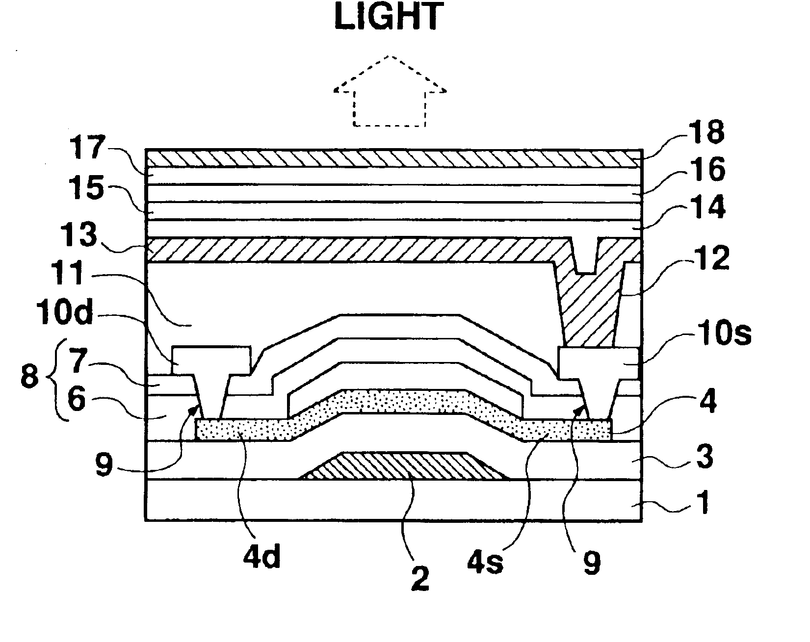
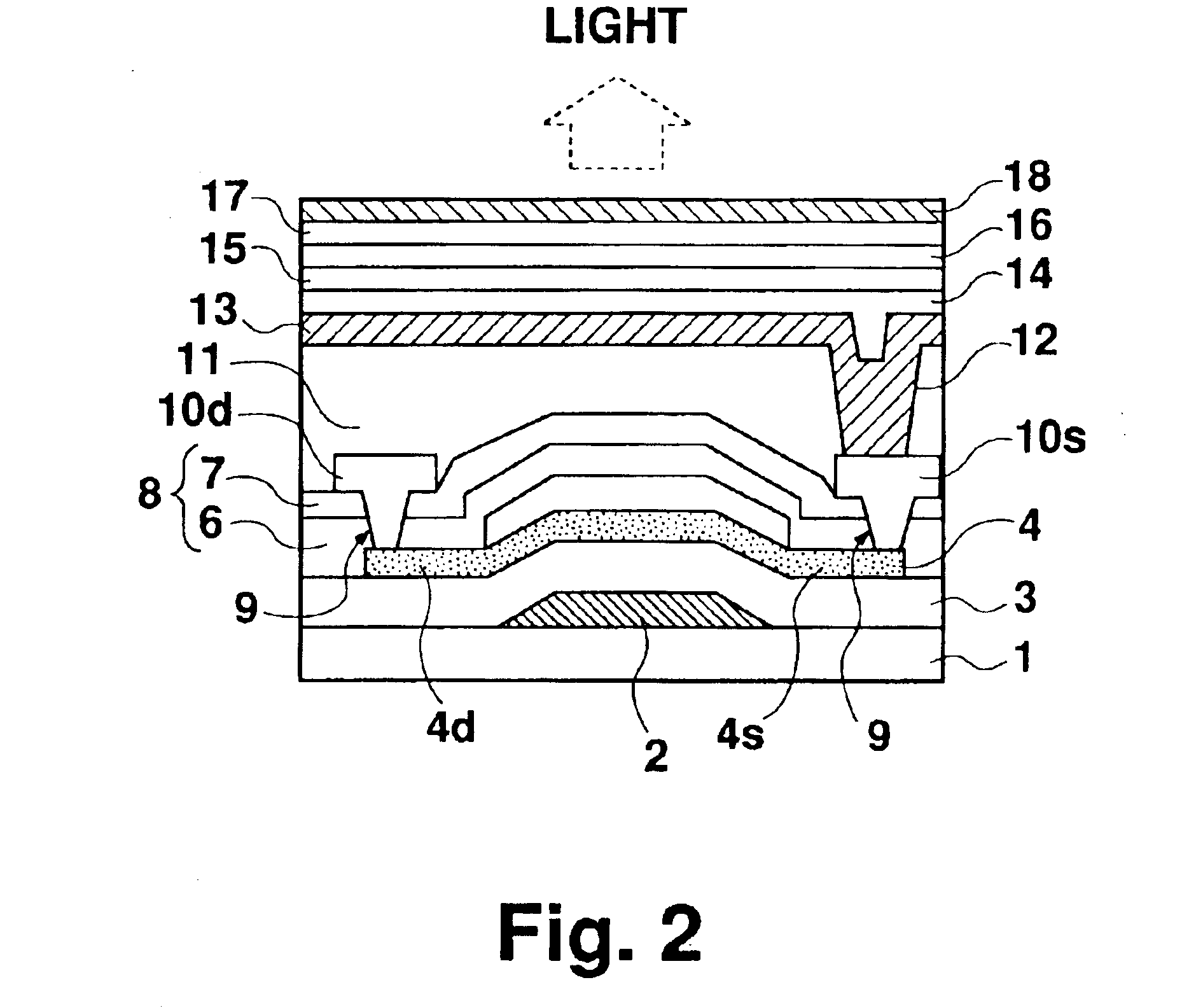
[0030]FIG. 2 is a cross sectional view illustrating one pixel of a display apparatus having organic EL elements and TFT elements, according to the present applicant.

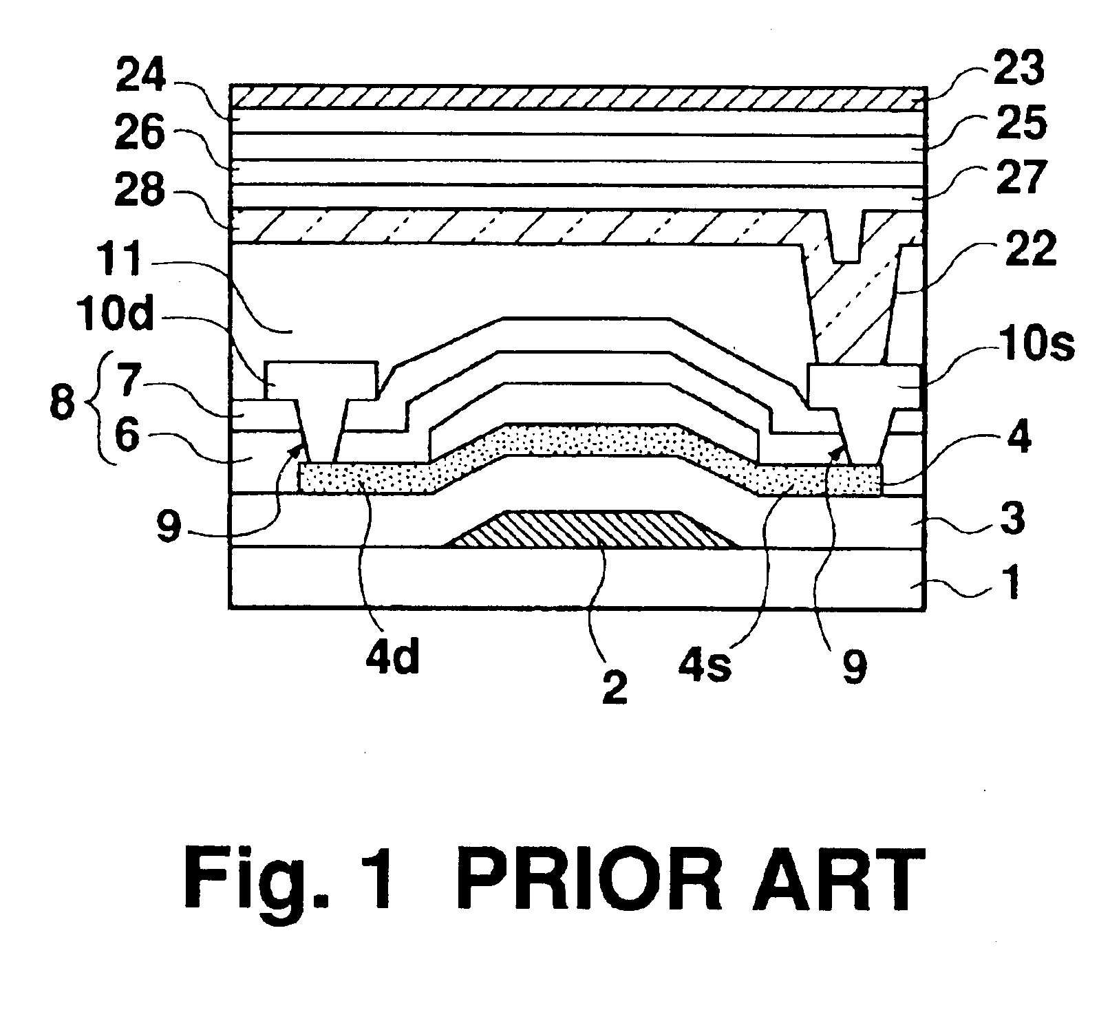
[0031]The display apparatus shown in FIG. 2 differs from that shown in FIG. 1 in that the TFT element and the organic element are reversely formed on the substrate 1.

[0032]In each display pixel, an TFT element and an organic EL element are laminated over an insulating substrate which is made of glass synthetic resin, or a conductive substrate or a semiconductor substrate on which an insulating film such as SiO2 film or SiN film is formed. The substrate 1 may be a transparent or opaque substrate.

[0033]The TFT structure formed on the substrate 1 is the same as that of the conventional TFT structure, and so repeated explanation will be omitted here. The source electrode 10s is c...


PUM


Abstract

A display apparatus includes display pixels each having a thin film transistor and an EL element formed successively forming over a substrate. The EL element has a cathode electrode connected to the source of the thin film transistor and an anode electrode, and is driven by the thin film transistor. The EL element externally emits light from the reverse side of the substrate. For example, when the cathode electrode is formed the comblike, meshlike, or gridlike pattern on the luminous layer, the light is emitted through the slits of the cathode pattern. The display apparatus is provided that can improve the aperture ratio of a display pixel and can increase the degree of freedom in deciding the size and the drive capability of a TFT element which drives an EL element.

Description

CROSS REFERENCE TO RELATED APPLICATIONS[0001]This application is a continuation application of U.S. patent application Ser. No. 09 / 258,499, filed on Feb. 26, 1999 now U.S. Pat. No. 6,630,784, and which is herein incorporated by reference in its entirety.BACKGROUND OF THE INVENTION[0002]1. Field of the Invention[0003]The present invention relates to a display apparatus that includes electroluminescence (hereinafter referred to as EL) elements and thin film transistors (hereinafter referred to as TFTs) which are fabricated on a substrate, and also to a method of fabricating the same.[0004]2. Description of the Related Art[0005]Recently, display apparatus using TFT elements and EL elements such as organic EL elements have been noted as display devices, in place of the CRTs (Cathode Ray Tubes) or LCD (Liquid Crystal Display) apparatus.[0006]FIG. 1 is a cross sectional view illustrating a conventional display apparatus including organic EL elements and TFT elements. FIG. 1 shows a lamina...

Claims


Application Information

Patent Timeline
Patent Type & Authority Patents(United States)
IPC IPC(8): H01L27/32H01L27/28H01L51/52H01L51/50H05B33/10G09F9/30H05B33/12H05B33/26
CPCH01L27/3244H01L27/3248H01L51/5203H01L51/5206H01L2251/5315H01L2251/5353H10K59/123H10K59/12H10K50/813H10K2102/321H10K2102/3026H01L31/12
Inventor YONEDA, KIYOSHI
Owner SANYO ELECTRIC CO LTD
Why Eureka
Try Eureka