Methods for forming chalcogenide glass-based memory elements

a technology of chalcogenide glass and memory elements, applied in the direction of basic electric elements, electrical equipment, semiconductor devices, etc., can solve the problems of difficult and complicated fabrication of pcram elements containing only glass with an open matrix used by itself,

Inactive Publication Date: 2005-10-11
MICRON TECH INC
View PDF125 Cites 27 Cited by
  • Summary
  • Abstract
  • Description
  • Claims
  • Application Information

AI Technical Summary

Problems solved by technology

While a PCRAM element comprised exclusively of a glass with an open matrix will be placed in a low resistance state or a high resistance state more quickly than a PCRAM element comprised exclusively of a glass with a tight matrix, glass with an open matrix used by itself is also not ideal.
Furthermore, the low melting point of selenium-rich glass, i.e., glass with an open matrix makes fabrication of PCRAM elements containing only glass with an open matrix difficult and complicated.

Method used


Image

  • Methods for forming chalcogenide glass-based memory elements
  • Methods for forming chalcogenide glass-based memory elements
  • Methods for forming chalcogenide glass-based memory elements

Examples


first embodiment

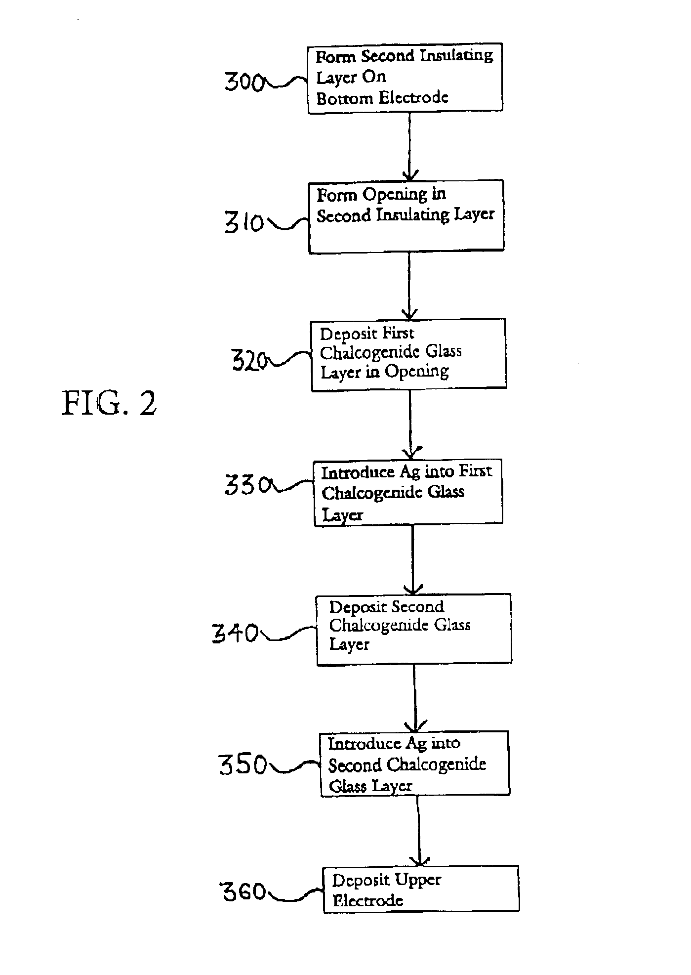
[0042]Using the FIG. 3 structure containing bottom electrode 56 as a starting point and referring to the processing sequence shown in FIG. 2, the invention will now be explained. At step 300 in FIG. 2, a second insulating layer 58 is formed over bottom electrode 56, as shown in FIG. 3. The second insulating layer 58 may comprise the same materials as first insulating layer 54, such as SiO2 and Si3N4. At step 310 an opening 60 is formed in second insulating layer 58 to provide the structure shown in FIG. 4. Opening 60 may be formed by known methods in the art, such as a conventional patterning and etching process. Opening 60 is formed such that the surface of bottom electrode 56 is exposed in opening 60. After the patterning and etch back process any masking material used is stripped away to leave the structure at a state represented in FIG. 4.

[0043]At step 320 a first chalcogenide glass, preferably a germanium-selenide glass layer 62, is formed in opening 60 on top of bottom electro...

second embodiment

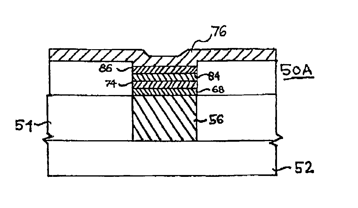
[0056]Referring now to FIG. 12, the present invention includes forming at least one additional silver-containing germanium-selenide glass layer above second silver-containing germanium-selenide glass layer 74. This is accomplished in the same way that second silver-containing germanium-selenide glass layer 74 is formed over first silver-containing germanium-selenide glass layer 68. Specifically, at step 350A, a chalcogenide glass, preferably an additional germanium-selenide glass layer 80, is deposited in opening 60 as shown in FIG. 13. This may be accomplished in the same ways that second germanium-selenide glass layer 70 is deposited at step 340. The additional germanium-selenide glass layer 80 preferably has a stoichiometry of GexSe100−x. The additional germanium-selenide glass layer 80 has a glass matrix structure distinct from any adjacently placed germanium-selenide glass layer, including second silver-containing germanium-selenide glass layer 74 in the case of a first additio...


PUM


Abstract

The present invention provides a design for a PCRAM element which incorporates multiple metal-containing germanium-selenide glass layers of diverse stoichiometries. The present invention also provides a method of fabricating the disclosed PCRAM structure.

Description

[0001]This application is a divisional of application Ser. No. 10 / 230,327, filed on Aug. 29, 2002 now U.S. Pat. No. 6,856,002, which is hereby incorporated by reference.BACKGROUND OF THE INVENTION[0002]1. Field of the Invention[0003]The invention relates to the field of random access memory (RAM) devices formed using chalcogenide glass layers, and in particular to an improved programmable conductor random access memory (PCRAM) element design utilizing germanium-selenide glass layers.[0004]2. Description of the Related Art[0005]Programmable conductor memory elements recently have been investigated for suitability as semi-volatile and non-volatile random access memory devices. One known PCRAM element composition utilizes a germanium-selenide chalcogenide glass of GexSe100−x stoichiometry. A metal, such as silver, is incorporated into the germanium-selenide glass. It is believed that the metal provides conductivity to the element thus allowing the element to be switched between two res...

Claims


Application Information

Patent Timeline
Patent Type & Authority Patents(United States)
IPC IPC(8): H01L45/00H01L21/8234H01L27/24
CPCH01L45/085H01L45/1233H01L45/143H01L45/1658H01L45/1683H10N70/245H10N70/826H10N70/8825H10N70/046H10N70/066
Inventor MOORE, JOHN T.GILTON, TERRY L.CAMPBELL, KRISTY A.
Owner MICRON TECH INC
Why Eureka
Try Eureka