Organic thin film transistor

a thin film transistor and organic technology, applied in the direction of organic semiconductor devices, organic chemistry, thermoelectric devices, etc., can solve the problems of restricting the application and structure of organic transistors, and achieve the effect of improving electrical conta

Inactive Publication Date: 2005-10-11
LG CHEM LTD
View PDF3 Cites 60 Cited by
  • Summary
  • Abstract
  • Description
  • Claims
  • Application Information

AI Technical Summary

Benefits of technology

[0013]The present invention further provides a method for manufacturing an organic transistor which comprises inserting an organic layer between a semi-conducting layer and source or drain electrode

Problems solved by technology

However, high work metals, which are novel metals, are expensive and hard to process using

Method used


Image

  • Organic thin film transistor
  • Organic thin film transistor
  • Organic thin film transistor

Examples


example 1

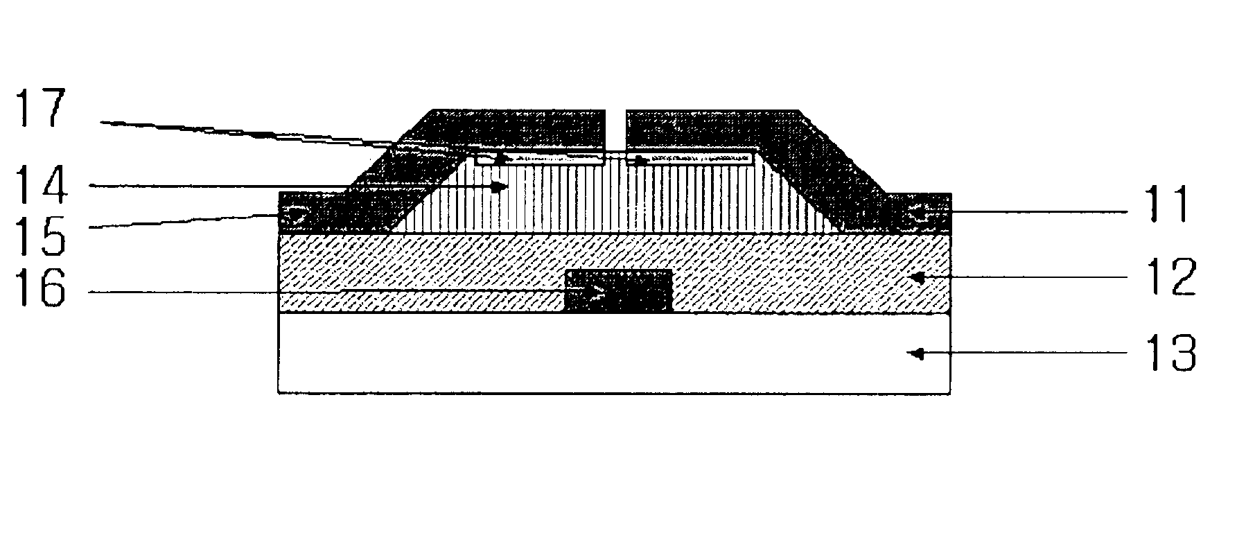
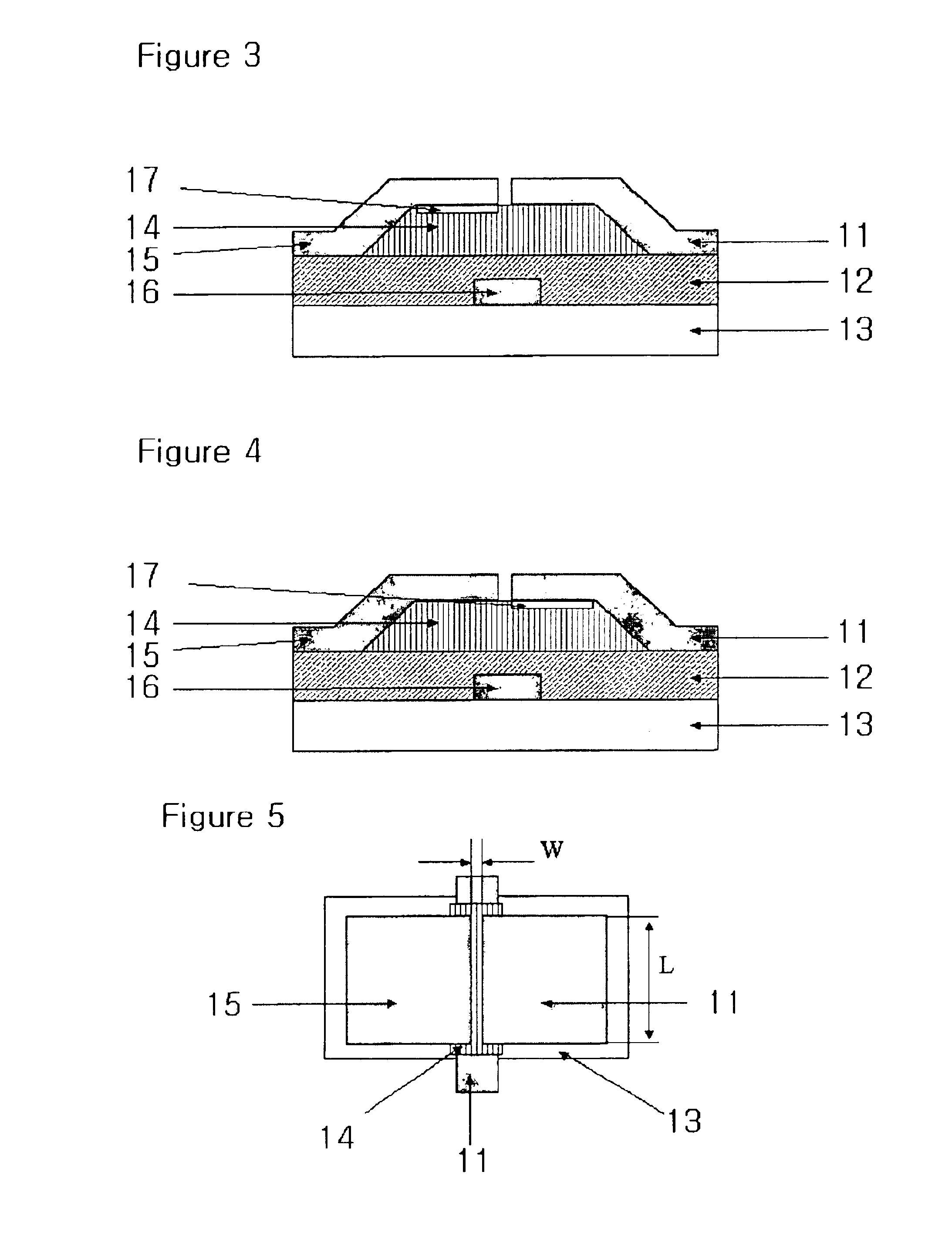
[0045]The field-effect transistors were fabricated in a staggered-inverted structure as shown in FIGS. 2 and 5. An ITO glass was used as the substrate 13. An ITO electrode is patterned as a gate electrode 16. The gate dielectric or insulator layer 12 was prepared by spin-coating the poly-4-vinylphenol (PVP) solution (15 wt % in propylene glycol monomethyl ether acetate (PGMEA)) at 2000 rpm and curing at 200° C. for 2 hours. The thickness of the PVP gate insulator was 922 nm. The semi-conducting layer 14 is formed on top of the PVP gate dielectric layer 12. Pentacene is used as a p-type semi-conducting materials. Pentacene semi-conducting layer 14 was deposited with a rate of 0.5 Å / s under the base pressure of 1×10⁻⁶ Torr. The thickness of pentacene layer is 100 nm. The organic layer 17 and gold (Au) source / drain electrodes 15 and 11, respectively, were deposited on top of the pentacene film through a shadow mask as shown in FIG. 2. The organic layer 17 was deposited on top of the pe...

example 2

[0047]The device was fabricated the same way as described in Example 1 except for replacing Au with Al as source / drain electrodes.

[0048]A graph illustrating the drain-source current (IDS) versus drain-source voltage (VDS) characteristics for several gate voltages (VG) is shown in FIG. 8. A graph illustrating the (IDS)1 / 2 versus VG characteristics for pentacene transistors (VDS=−50V) is shown in FIG. 12. In the saturation regime of the drain-source current, the field-effect mobility is calculated as μFET=0.18 cm2 / Vs.


PUM


Abstract

An organic transistor including an organic layer is provided. The organic layer includes at least one compound represented by the Chemical Formula I.

Description

CROSS REFERENCE TO RELATED APPLICATIONS[0001]This application is a continuation-in-part claiming priority to U.S. patent application Ser. No. 09 / 914,731, filed Aug. 30, 2001, now U.S. Pat. No. 6,720,573, PCT filed on Dec. 27, 2000, which is based on application No. 10-1999-067746 and No. 10-2000-82085 filed in the Korean Industrial Property Office on Dec. 31, 1999 and Dec. 26, 2000, respectively, the content of which is incorporated hereinto by reference.BACKGROUND OF THE INVENTION[0002]1. Field of the Invention[0003]The present invention relates to new organic materials used in organic transistors. More particularly, the present invention pertains to novel organic compounds facilitating the ohmic contact between semi-conducting layer and electrodes and use in organic thin film transistors.[0004]2. Description of the Related Art[0005]Thin film field-effect transistors (FETs) comprise the basic building blocks for microelectronics. A FET has three electrodes (e.g., source, drain, and...

Claims


Application Information

Patent Timeline
IPC IPC(8): C07D487/14C07D487/00H01L51/05H01L51/30H01L51/52H01L51/50C07D487/12H01L35/24
CPCC07D487/14H01L51/0072H01L51/0076H01L51/0545H01L51/0562H01L51/0541H01L51/0055H01L2251/308H01L51/5012H01L51/5203H10K85/623H10K85/6572H10K85/731H10K10/464H10K10/466H10K10/486H10K50/11H10K2102/103H10K50/805
Inventor SON, SE-HWANYOON, SEOKHEECHOI, HYEONLEE, CHANGHEE
Owner LG CHEM LTD
Why Eureka
Try Eureka