CMOS inspection apparatus

a technology of inspection apparatus and microscope, which is applied in the field of system and method of inspection of semiconductor devices, can solve the problems of image distortion, slow image processing speed, and inability to apply component inspection systems

Inactive Publication Date: 2005-10-25
ASTI HLDG +1
View PDF5 Cites 24 Cited by
  • Summary
  • Abstract
  • Description
  • Claims
  • Application Information

AI Technical Summary

Benefits of technology

[0009]Those skilled in the art will further appreciate the advantages and superior features of the invention together with other important aspects thereof on reading the detailed description that follows in conjunction with the drawings.

Problems solved by technology

Although such CMOS imaging systems are known in the art, they have not been applied to component inspection systems.
One reason why such CMOS imaging systems have not been used is because the speed of image processing is slower than equivalent systems and methods, such as systems utilizing Charge Coupled Devices (CCDs) or methods requiring operator review of image data.
In addition, earlier attempts to increase camera speed resulted in image distortion.
Other problems have also been encountered, such as poor image quality that rendered the pixel data generated by the CMOS sensor unusable.
Thus, although CMOS sensors have been applied for various imaging applications, the application of CMOS sensors for component inspection has not been accomplished because of these problems.

Method used


Image

  • CMOS inspection apparatus
  • CMOS inspection apparatus
  • CMOS inspection apparatus

Examples


Embodiment Construction

[0016]In the description that follows, like parts are marked throughout the specification and drawings with the same reference numerals, respectively. The drawing figures might not be to scale, and certain components can be shown in generalized or schematic form and identified by commercial designations in the interest of clarity and conciseness.

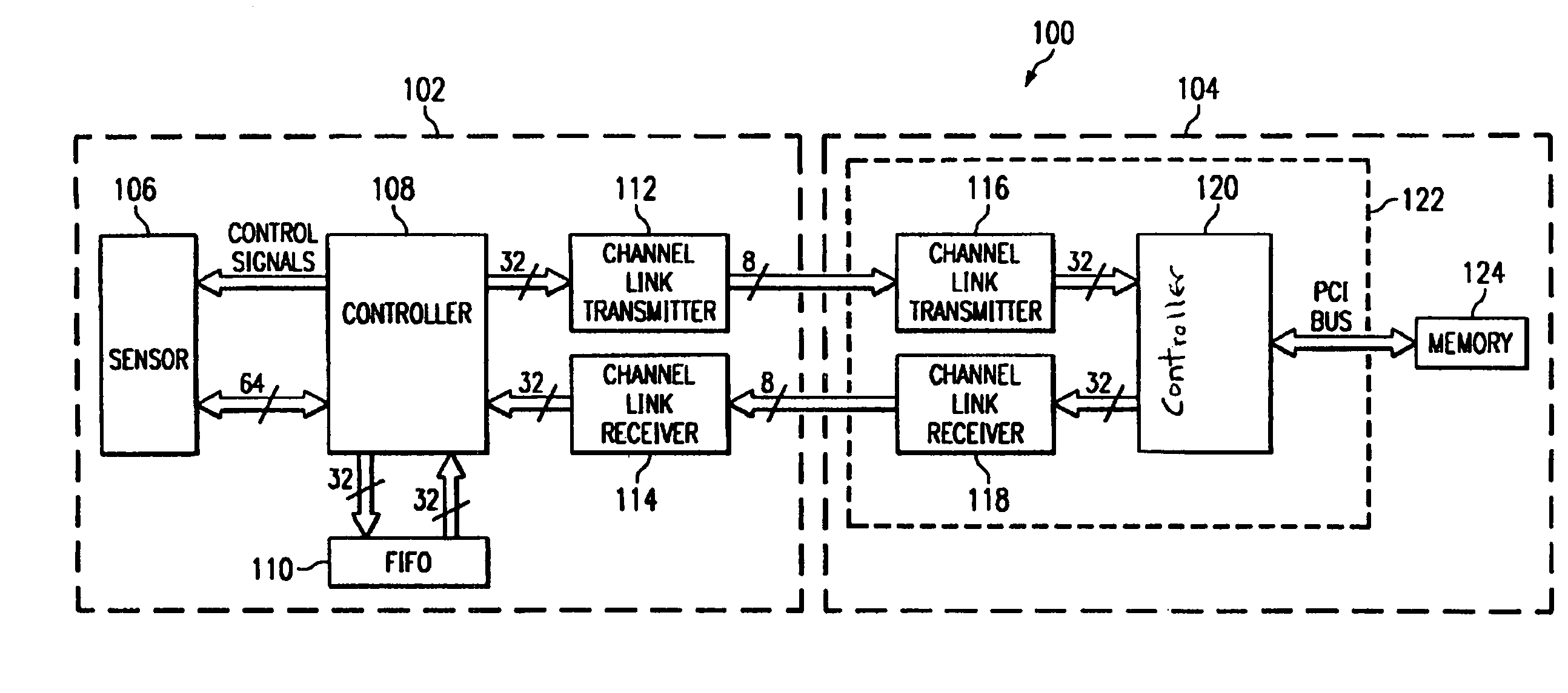
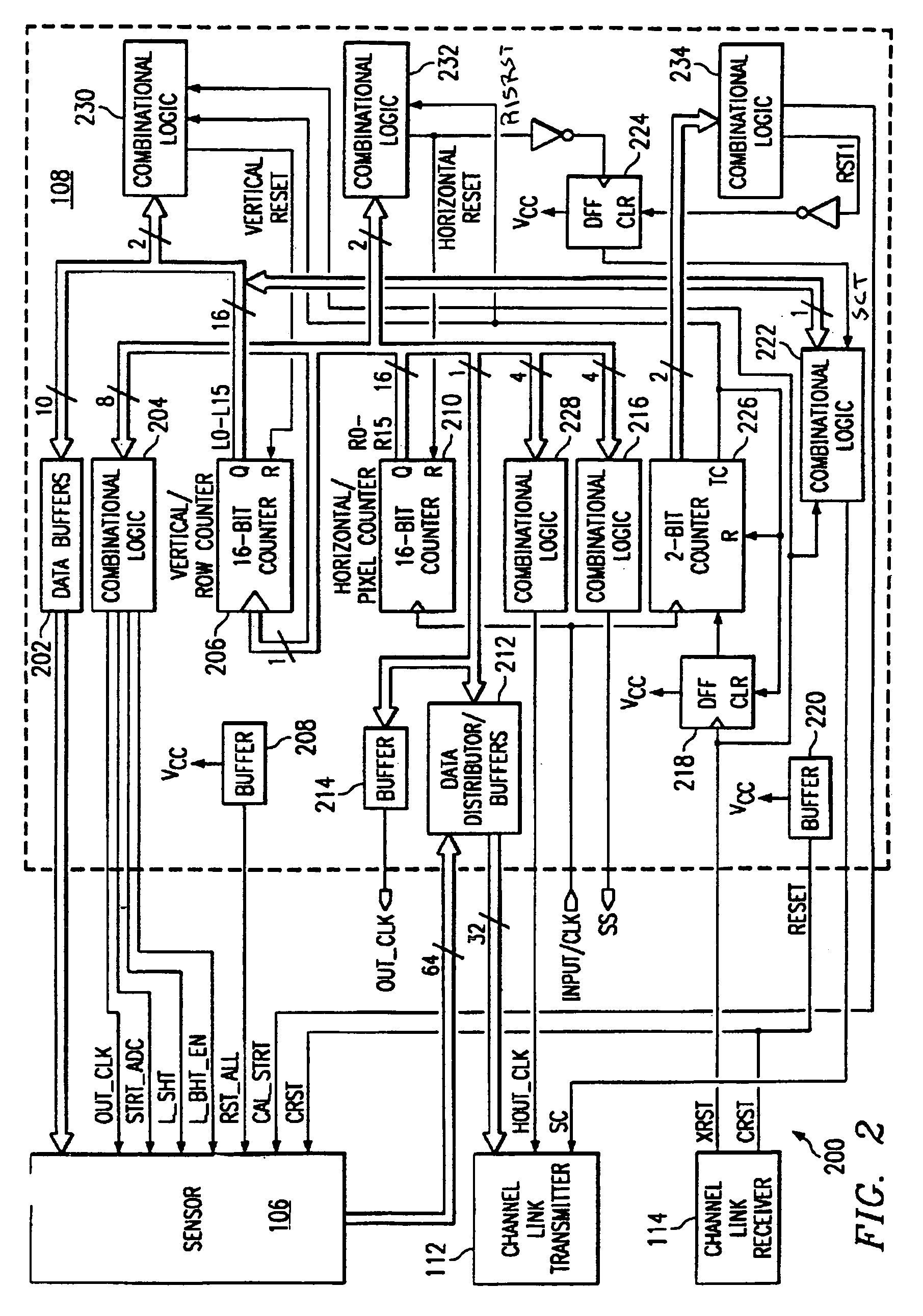
[0017]FIG. 1 is a diagram of system 100 for performing component inspection using CMOS imaging in accordance with an exemplary embodiment of the present invention. System 100 uses a CMOS sensor and dedicated processing circuitry to increase the speed of image processing so that the CMOS sensor can be used to generate component inspection image data for commercial applications.

[0018]System 100 includes digital camera 102, which is coupled to processor 104. As used herein, the term “couple” and its cognate terms such as “couples” and “coupled” can include a physical connection (such as through a copper conductor), a virtual connection (such as...


PUM


Abstract

A system for inspecting components is provided. The system includes a CMOS imaging system generating image data, such as pixel data from a pixel array. An image analysis system is connected to the CMOS imaging system, the image analysis system receiving the image data and generating image analysis data. The CMOS imaging system generates the image data at a rate that allows the CMOS imaging device to be used for inspecting components.

Description

FIELD OF THE INVENTION[0001]The present invention pertains to the field of semiconductor devices, and more particularly to a system and method for inspecting semiconductor devices that uses CMOS image data acquisition.BACKGROUND[0002]Complementary metal-oxide semiconductor (CMOS) imaging systems are known in the art. Such CMOS imaging systems use CMOS devices having an array of picture elements (pixels) to generate digital image data. The digital image data from such CMOS devices is then processed and stored, such that the image can be recreated from the stored pixel data.[0003]Although such CMOS imaging systems are known in the art, they have not been applied to component inspection systems. One reason why such CMOS imaging systems have not been used is because the speed of image processing is slower than equivalent systems and methods, such as systems utilizing Charge Coupled Devices (CCDs) or methods requiring operator review of image data. In addition, earlier attempts to increa...

Claims


Application Information

Patent Timeline
Patent Type & Authority Patents(United States)
IPC IPC(8): H04N5/335
CPCH04N5/335H04N25/00
Inventor RAO, SREENIVASJUSOH, NOOR ASHEDAH BINTI
Owner ASTI HLDG
Why Eureka
Try Eureka