Display device

a technology of a display device and a display screen, which is applied in the direction of radiation control devices, identification means, instruments, etc., can solve problems such as accumulation of damage, and achieve the effects of reducing the influence of plasma damage, and small luminance variation

Inactive Publication Date: 2005-11-01
SEMICON ENERGY LAB CO LTD
View PDF79 Cites 63 Cited by
  • Summary
  • Abstract
  • Description
  • Claims
  • Application Information

AI Technical Summary

Benefits of technology

[0008]The present invention has been made in view of the above-mentioned problems and an object of the present invention is to provide a device structure effective in reducing an influence of plasma damage in a manufacturing process of a display device. Further, another object of the present invention is to provide a display device having uniform display characteristics (referring to display characteristics small in luminance variation between adjacent pixels and in degradation degree) obtained by reducing the influence of the plasma damage to suppress variations in threshold voltage of transistors.
[0024]Note that the planarization layer of the present invention may be formed of either an inorganic insulating film or an organic resin film formed by sputtering, plasma CVD, low-pressure thermal CVD, or spin-coating. Also, when the planarization layer is formed by sputtering, plasma CVD, or low-pressure thermal CVD, its surface may be polished before the use (inclusive of polishing with a mechanical or chemical action, or a combined action thereof). By using the planarization layer, the surface of a first electrode formed on the planarization layer can be leveled and the light emitting element (EL element) can be prevented from being short-circuited. Also, by providing the barrier layer thereon, impurity diffusion from the EL element can be blocked to protect TFTs and degassing from an organic insulating film can be avoided as well. Further, by forming the barrier layer in the portion close to the active layer of the TFT, the impurity diffusion from the EL element is blocked to effectively protect the TFT.(2) A display device according to the present invention includes:
[0148]Further, according to the structures stated in (7), (8), and (9), the pixel electrode is connected with the drain electrode through a contact hole and insulated from the other wirings through the planarization layer, so that the area of the pixel electrode can be increased.
[0149]Note that, according to the structures stated in (7) to (9), the upper surface of the planarization layer may be covered with the silicon nitride film. This is because when the organic resin film is used as the planarization layer, in particular, the upper surface thereof (including an inner wall surface thereof when any opening is formed) is covered with the silicon nitride film, so that gases (including a component gas or moisture) generated from the organic resin film can be effectively prevented from diffusing to the light emitting element side.
[0200]In the above structures of the present invention, the silicon nitride film used for the barrier layer is preferably made as fine as possible. The higher the finess, the higher the barrier property. The diffusion blocking effect against the degassing component is thus enhanced. For example, when the organic resin film is used as the planarization layer, the diffusion of the component gas or moisture therefrom to the transistor side or the light emitting element side can be effectively suppressed.

Problems solved by technology

In other words, in order to achieve a highly reliable display device, attention must be paid not only to an influence of an accumulated damage in the process during manufacturing the device but also to the subsequent deterioration with time, which results from the accumulated damage.

Method used


Image

  • Display device
  • Display device
  • Display device

Examples


embodiment 1

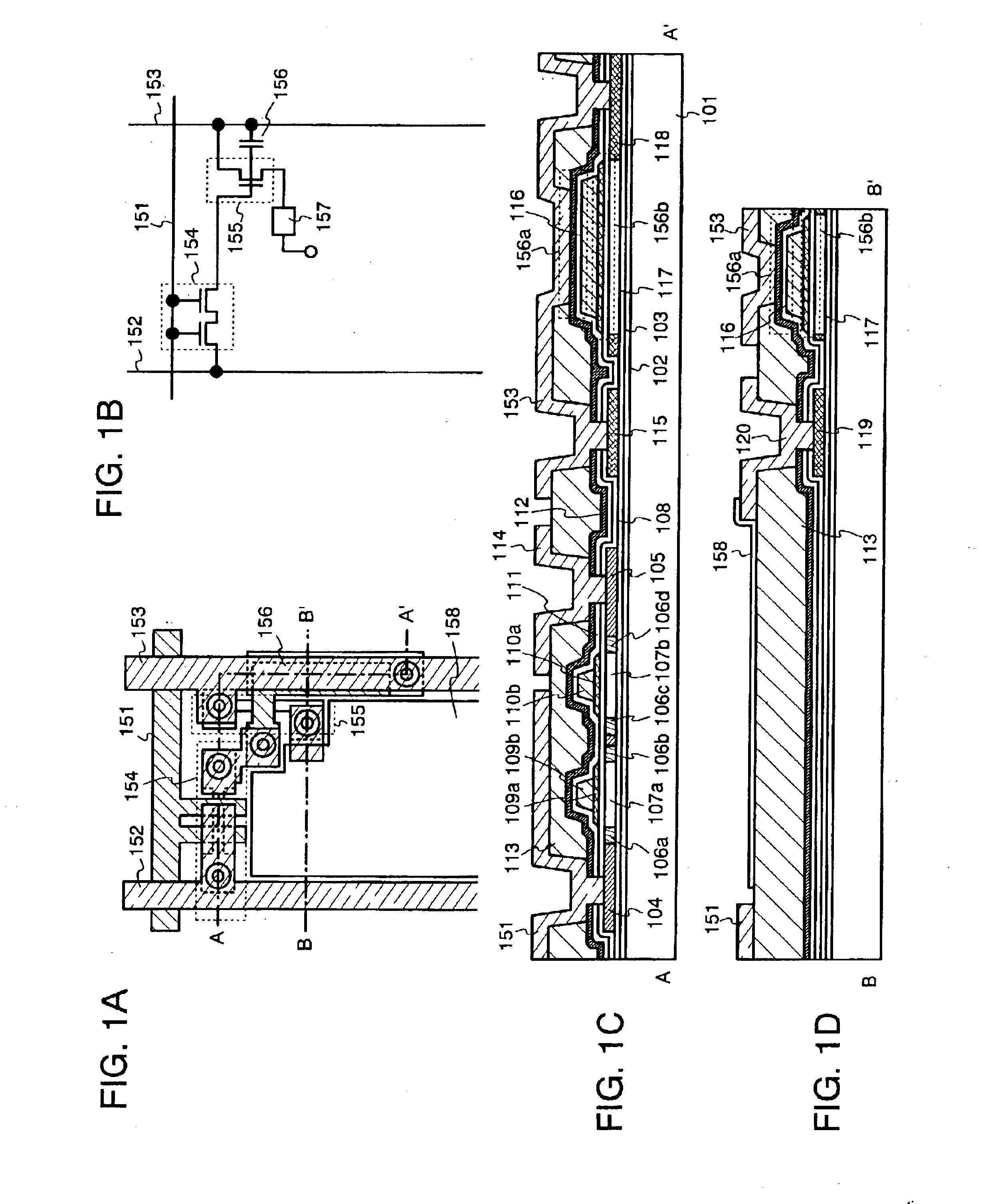
[0232]In this embodiment, an example of an electroluminescence display device of the present invention will be described. FIG. 1A is a top view of a pixel of the electroluminescence display device (note that a state up to the formation of a pixel electrode is indicated), FIG. 1B is a circuit diagram thereof, and FIGS. 1C and 1D each are a cross sectional view along a line A-A′ or B-B′.

[0233]As shown in FIGS. 1A and 1B, a pixel portion of the electroluminescence display device includes a plurality of pixels which are surrounded by gate wirings 151, data wirings 152, and power source wirings (wirings for supplying a constant voltage or a constant current) 153 and arranged in matrix. In each of the pixels, a TFT 154 serving as a switching element (hereinafter referred to as a switching TFT), a TFT 155 serving as means for supplying a current or a voltage for producing light emission of an light emitting element (hereinafter referred to as a driver TFT), a capacitor portion 156, and an ...

embodiment 2

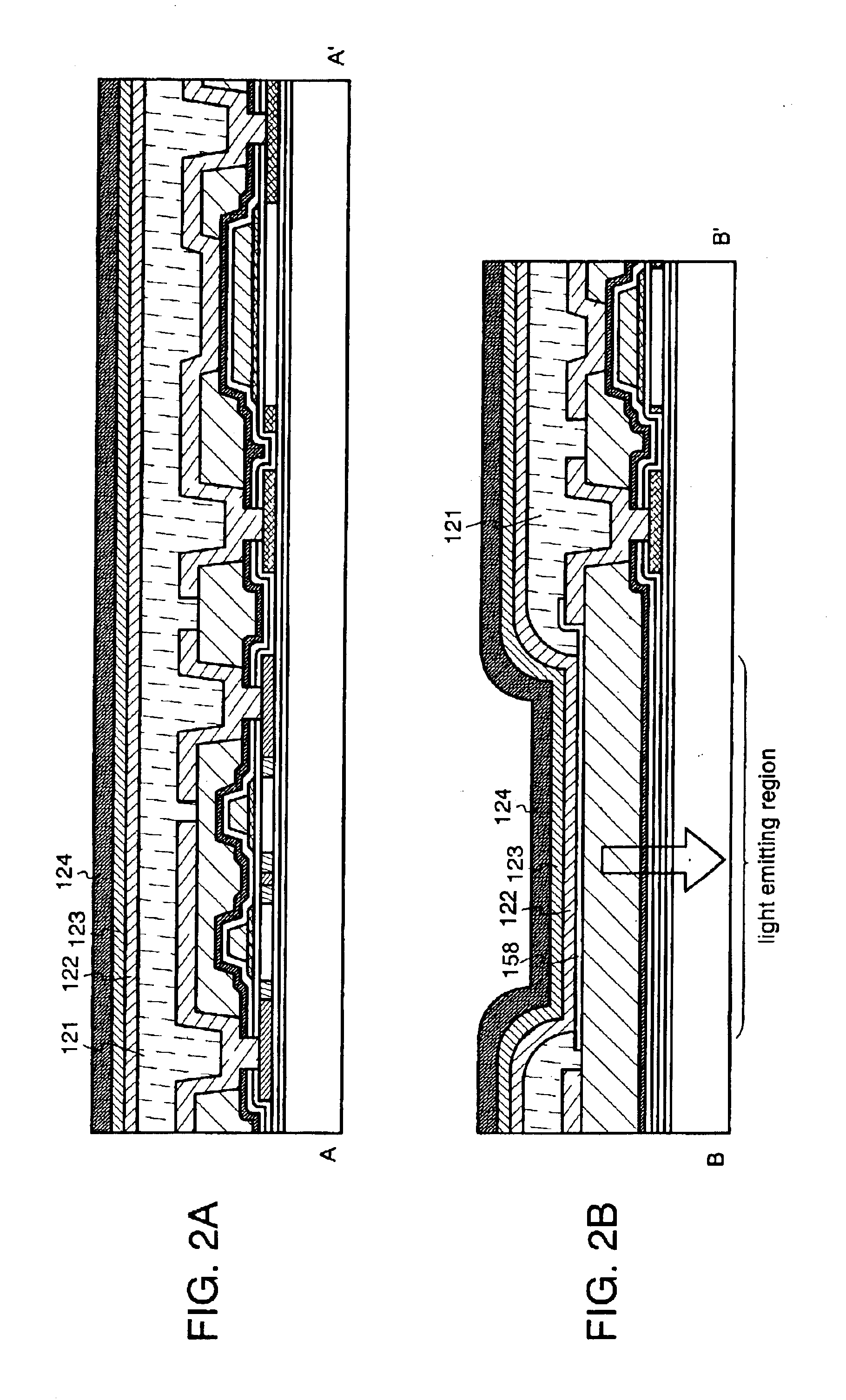
[0251]In this embodiment, description will be given of an example of a device structure including the one in which a planarization layer and a barrier layer are reversed in position in Embodiment 1. Other structures thereof are the same as those in Embodiment 1 and thus, may be attained referring to the description of Embodiment 1. Accordingly, this embodiment will be described focusing on the point different from Embodiment 1.

[0252]FIGS. 3A and 3B are views corresponding to FIGS. 2A and 2B in Embodiment 1, respectively. In the figures, some components are denoted by the same reference symbols as those in Embodiment 1. In this embodiment, a planarization layer 301 is formed on an insulating layer 111 and a second opening is formed on the planarization layer 301, after which a barrier layer 302 is formed so as to cover a top surface of the planarization layer 301 and a side surface (inner wall surface) of the second opening. Further, inside the second opening, a gate insulating film ...

embodiment 3

[0254]In this embodiment, description will be given of an example of a device structure including the one in which a planarization layer and a barrier layer are reversed in position in Embodiment 1. Other structures thereof are the same as those in Embodiment 1 and thus, may be attained referring to the description of Embodiment 1. Accordingly, this embodiment will be described focusing on the point different from Embodiment 1.

[0255]FIGS. 4A and 4B are views corresponding to FIGS. 2A and 2B in Embodiment 1, respectively. In the figures, some components are denoted by the same reference symbols as those in Embodiment 1. In this embodiment, a planarization layer 401 is formed on an insulating layer 111 and a barrier layer 402 is formed thereon, after which the barrier layer 302, planarization layer 401, insulating layer 111, and a gate insulating film 108 are etched to form an opening.

[0256]With the structure of this embodiment, degassing from the planarization layer 401 can be suppre...


PUM


Abstract

A display device according to the present invention includes: a planarization layer for insulating between a gate electrode etc. and a data wiring, a drain electrode, or the like of the transistor; and a barrier layer that is formed on an upper surface or lower surface of the planarization layer and at the same time, adapted to suppress diffusion of moisture or degassing components from the planarization layer. The display device adopts a device structure effective in reducing the plasma damage on the planarization layer by devising a positional relationship between the planarization layer and the barrier layer. Also, in combination with a novel structure as a structure for a pixel electrode, effects such as an increase in luminance can be provided as well.

Description

BACKGROUND OF THE INVENTION[0001]1. Field of the Invention[0002]The present invention belongs to a technical field related to a display device in which a semiconductor device (typically, a transistor) is used as a device, in particular, a light emitting device represented by an electroluminescence display device, and to a technical field related to an electronic apparatus equipped with the display device in an image display portion.[0003]2. Description of the Related Art[0004]In recent years, development of liquid crystal display devices and electroluminescence display devices in which transistors (particularly, thin film transistors) are integrated on a substrate have progressed. Such. display devices are respectively characterized in that the transistors are formed on a glass substrate by using a thin film formation technique, and the transistors thus formed are disposed in pixels each arranged in matrix and made to function as a display device for image display.[0005]A variety of...

Claims


Application Information

Patent Timeline
Patent Type & Authority Patents(United States)
IPC IPC(8): H01L29/786H01L29/66H01L29/04H01L21/00H01L31/18H01L29/02H01L31/0264H01L31/0336H01L31/036H01L31/0376H01L31/20H05B33/14G09F9/30H01L21/336H01L27/32H01L51/50H05B33/12H05B33/22
CPCH01L27/3244H01L27/3258H01L27/1214H01L27/1248H01L27/3246H01L27/326H01L51/5271H01L2251/5315H01L51/5237H10K59/124H10K59/121H10K59/122H10K59/12H10K50/841H10K50/856H10K50/844H10K2102/3026H05B33/00H10K59/1213H10K50/84H01L29/4958H01L29/4966H01L29/78645H01L27/124H01L27/1255
Inventor YAMAZAKI, SHUNPEIMURAKAMI, SATOSHIOSAME, MITSUAKI
Owner SEMICON ENERGY LAB CO LTD
Why Eureka
Try Eureka