Fingerprint detection device and method of its manufacture, and apparatus for forming a protective film

a fingerprint detection and fingerprint technology, applied in the field of fingerprint detection devices, can solve the problems that cannot be applied to fingerprint detection devices, and achieve the effect of improving the strength of the surface and the ability to withstand the voltage of the electrostatic discharge of the semiconductor chip

Inactive Publication Date: 2005-11-01
SONY CORP
View PDF4 Cites 34 Cited by
  • Summary
  • Abstract
  • Description
  • Claims
  • Application Information

AI Technical Summary

Benefits of technology

[0016]Thus, the strength of the surface and the electrostatic discharge withstand voltage of the fingerprint detectable semiconductor chip can be improved without any cover. Moreover, the DLC film prevents the surface from being scratched and stained. Since a conventional protective cover is not needed, the fingerprint detection device can be given in a thin and compact form. The device also acquires high reliability.
[0018]In the second fingerprint detection device, because a carbon based protective film is covered over the entire area of the semiconductor chip in the window section defining the fingerprint detection area and also on insulating film on a peripheral of the window section, the strength of the surface and the electrostatic discharge withstand voltage of the fingerprint detectable semiconductor chip can be improved without any protective cover. Particularly, the carbon based protective film also reinforces the insulating film on a periphery of the window section. This permits provision of a further reliable fingerprint detection device.
[0020]In the first method of manufacturing a fingerprint detection device, the strength of the surface and the electrostatic discharge withstand voltage of the semiconductor chip are improved without any protective cover, which enables production of a highly reliable fingerprint detection device.
[0022]In the second method of manufacturing a fingerprint detection device, the strength of the surface and the electrostatic discharge withstand voltage of the semiconductor chip can be also improved without any protective cover. Particularly, the carbon based protective film also reinforces the insulating film on a periphery of the window. This permits manufacturing a reliable fingerprint detection device. It is noted that a step of processing a protective film for the surface can be omitted.

Problems solved by technology

However, they cannot be applied to the fingerprint detection device since diamond film is formed at a temperature in the range from 800 to 1000° C., far above the melting point of aluminum lead wires used in the fingerprint detection device.

Method used


Image

  • Fingerprint detection device and method of its manufacture, and apparatus for forming a protective film
  • Fingerprint detection device and method of its manufacture, and apparatus for forming a protective film
  • Fingerprint detection device and method of its manufacture, and apparatus for forming a protective film

Examples


first embodiment

(1) First Embodiment

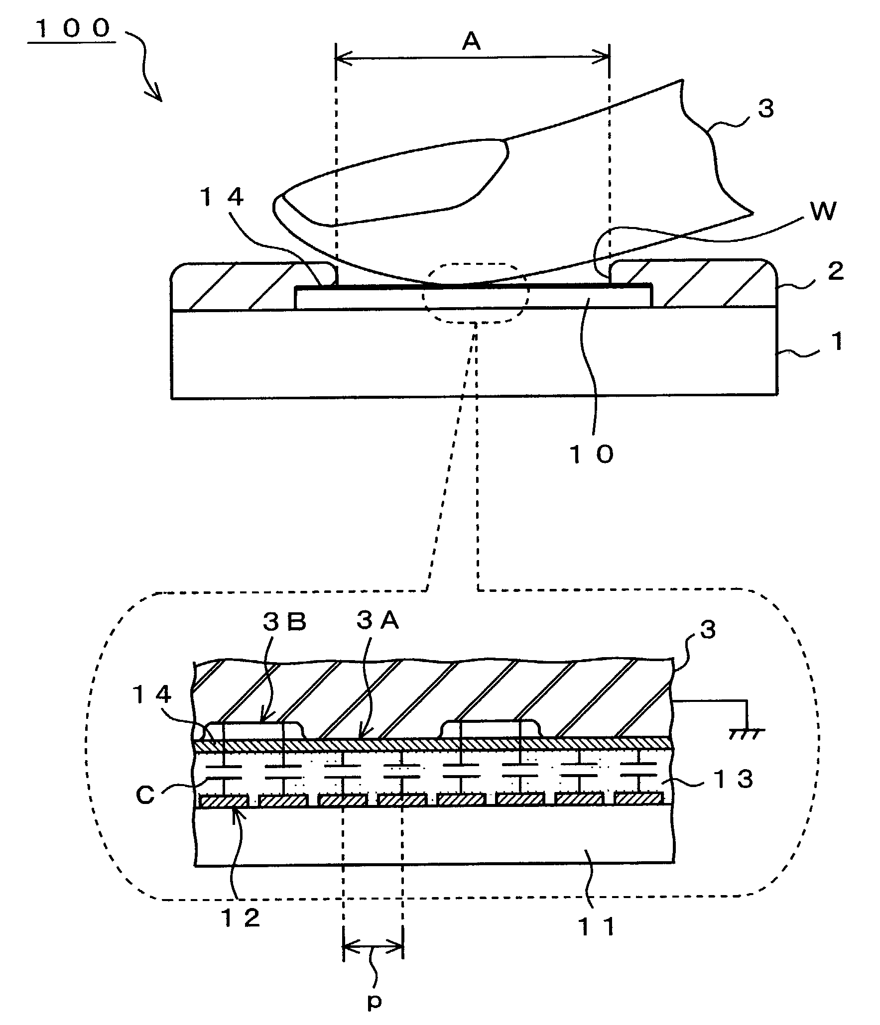
[0051]FIGS. 1A and 1B respectively show a side elevation view of a first embodiment of a fingerprint detection device and an enlarged cross sectional view of a portion thereof according to the invention. In this embodiment, the protective DLC film is formed on the outermost surface of the fingerprint detectable semiconductor chip so that the strength of the surface and the electrostatic discharge withstand voltage of a fingerprint detectable semiconductor chip are improved without any protective cover.

[0052]A fingerprint detection device 100 shown in FIG. 1A as the first embodiment is designed to detect a fingerprint of person, comprising a fingerprint detectable semiconductor chip (hereinafter referred to as fingerprint sensor chip) 10 formed on a substrate 1. A carbon based protective film 14 is deposited on the outermost surface of the fingerprint sensor chip 10. The fingerprint sensor chip 10 has a fingerprint detection area A. The peripheral section of the p...

second embodiment

(2) Second Embodiment

[0090]FIGS. 5A and 5B respectively show a side elevation view of a second embodiment of a fingerprint detection device and an enlarged cross sectional view of a portion thereof according to the invention. In the second embodiment, a DLC film 14 as a protective film is formed over the entire surface of a fingerprint sensor chip 20 inside a window section W and on insulating film 2 on a peripheral of the window section W after the fingerprint sensor chip 20 is packaged.

[0091]A fingerprint detection device 200 shown in FIG. 5A as the second embodiment is designed to detect a fingerprint of person, comprising a fingerprint detectable semiconductor chip (hereinafter referred to as fingerprint sensor chip) 20 formed on a substrate 1. The fingerprint sensor chip 20 has a fingerprint detection area A, as in the first embodiment. Lying beneath the fingerprint detection area A are a multiplicity of sense electrodes 12 arranged in a grid, and a silicon nitride film 13 form...


PUM

PropertyMeasurementUnit
thicknessaaaaaaaaaa
thicknessaaaaaaaaaa
temperatureaaaaaaaaaa

Abstract

A fingerprint detection device has a fingerprint sensor chip and a diamond-like carbon (DLC) film covering the outermost surface of the sensor chip. The DLC film provides sufficient strength and enhanced electrostatic discharge withstand voltage to the fingerprint sensor chip. Thus, the DLC film protects the fingerprint sensor chip without any conventional protective cover. The DLC film is less scratchable and less stainable. Since the fingerprint detection device has no protective cover, the device can be provided in a thin and compact form. In addition, the device has high reliability.

Description

[0001]This application claims priority to Japanese Patent Application Number JP2001-250607 filed Aug. 21, 2001 which is incorporated herein by reference.BACKGROUND OF THE INVENTION[0002]1. Field of the Invention[0003]The invention relates to a fingerprint detection device and a method of its manufacture. More particularly, the invention relates to a fingerprint detection device having a semiconductor chip for detecting a fingerprint (hereinafter referred to as fingerprint detectable semiconductor chip), the outermost upper surface of the semiconductor chip covered with a protective film of a carbon based material (the protective film hereinafter referred to as carbon based protective film) which can enhance the intensity of the surface and the electrostatic discharge withstand voltage of the semiconductor chip without any protective cover. The invention also relates to an apparatus for forming such protective film.[0004]2. Description of the Related Art[0005]In recent years, there a...

Claims


Application Information

Patent Timeline
Patent Type & Authority Patents(United States)
IPC IPC(8): G06K9/00G01B7/28C23C16/27G06T1/00
CPCG06K9/00053Y10S438/931Y10S257/914G06V40/1329
Inventor MIYAI, SEIICHIOKA, SHUICHI
Owner SONY CORP
Why Eureka
Try Eureka