Apparatus and methods for optically-coupled memory systems

a technology of optically coupled memory and apparatus, applied in the field of memory systems, can solve problems such as hammering the commercialization of optically-based system memories, and achieve the effect of free spa

Inactive Publication Date: 2005-11-01
ROUND ROCK RES LLC
View PDF12 Cites 55 Cited by
  • Summary
  • Abstract
  • Description
  • Claims
  • Application Information

AI Technical Summary

Benefits of technology

[0006]The present invention is directed to apparatus and methods for optically-coupled memory systems. In one aspect, a system memory includes a carrier substrate, and a controller attached to the carrier substrate and operable to transmit and receive optical signals, and first and second memory modules. The module substrate of the first memory module has an aperture formed therein, the aperture being adapted to provide an optical path for optical signals between the controller and an optical transmitter / receiver unit of the second memory module. Thus, the system memory provides the advantages of “free space” optical connection in a compact arrangement of memory modules.

Problems solved by technology

Problems of transmitting and receiving optical signals between the memory controller 50 and the memory modules 44, however, continue to hamper the commercialization of optically-based system memories, particularly those systems having an array of parallel, closely-spaced memory modules of the type found in many existing personal computer systems.

Method used


Image

  • Apparatus and methods for optically-coupled memory systems
  • Apparatus and methods for optically-coupled memory systems
  • Apparatus and methods for optically-coupled memory systems

Examples


Embodiment Construction

[0021]The present description is generally directed toward novel apparatus and methods for optically-coupled memory systems. Many specific details of certain embodiments of the invention are set forth in the following description and in FIGS. 3-11 to provide a thorough understanding of such embodiments. One skilled in the art will understand, however, that the present invention may have additional embodiments, or that the present invention may be practiced without several of the details described in the following description.

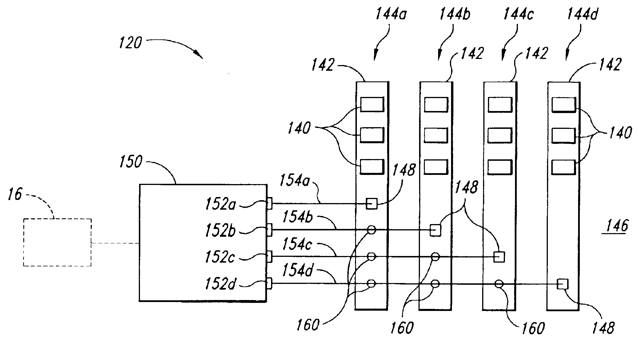
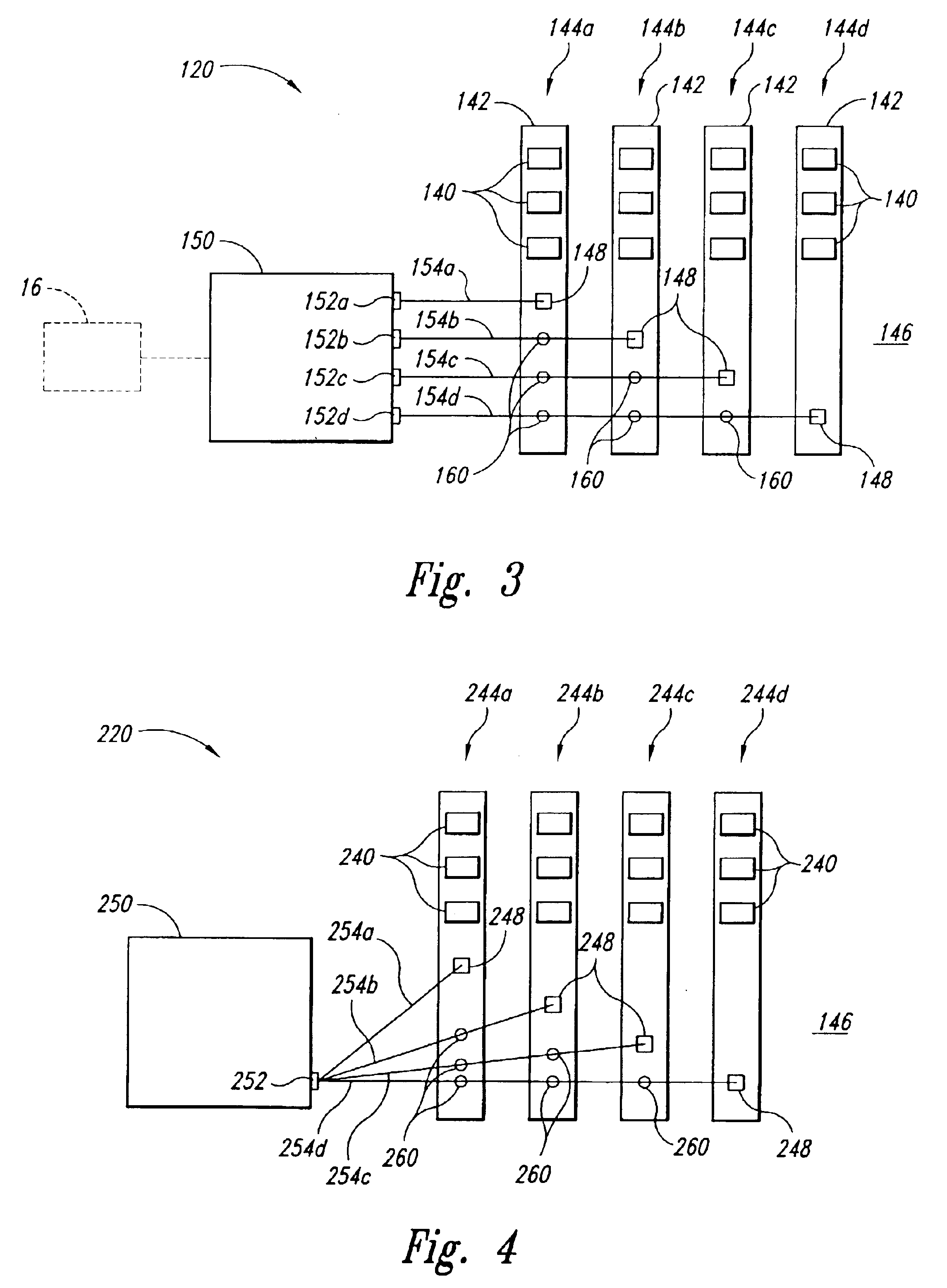
[0022]FIG. 3 is a top schematic view of a system memory 120 in accordance with an embodiment of the invention. For clarity, the system memory120 shown in FIG. 3 is not drawn to scale. The system memory 120 includes a plurality of memory modules 144 mounted on a carrier substrate (or motherboard) 146. The memory modules 144 may be removably plugged into the motherboard 146 in the conventional manner. Each memory module 144 includes a module substrate 142. As desc...


PUM


Abstract

Optically-coupled memory systems are disclosed. In one embodiment, a system memory includes a carrier substrate, and a controller attached to the carrier substrate and operable to transmit and receive optical signals, and first and second memory modules. The module substrate of the first memory module has an aperture formed therein, the aperture being operable to provide an optical path for optical signals between the controller and an optical transmitter / receiver unit of the second memory module. Thus, the system memory provides the advantages of “free space” optical connection in a compact arrangement of memory modules. In an alternate embodiment, the first memory module includes a beam splitter attached to the module substrate proximate the aperture. In another embodiment, the first and second memory modules are staged on the carrier substrate to provide an unobstructed path for optical signals. In another embodiment, the optical transmitter / receiver unit projects outwardly from the module substrate to provide an unobstructed path for optical signals.

Description

TECHNICAL FIELD[0001]The present invention relates to memory systems, and more particularly to novel apparatus and methods for optically-coupled memory systems.BACKGROUND OF THE INVENTION[0002]A conventional computer system 10 shown in FIG. 1 includes a central processing unit (“CPU”) 12, such as a microprocessor, that is coupled to a bus bridge 16, memory controller or the like. The CPU 12 is also typically coupled to a cache memory 18 to allow instructions and data to be more frequently accessed by the CPU 12. The bus bridge 16 allows the CPU 12 to receive program instructions from a system memory 20. The CPU 12 can also write data to and read data from the system memory 20 through the bus bridge 16. The CPU 12 also preferably transfers video data from the system memory 20 to a display system including a graphics processor or graphics accelerator 24, a video RAM 26, and a conventional display 28, such as a cathode ray tube (“CRT”), liquid crystal display (“LCD”) or field emission ...

Claims


Application Information

Patent Timeline
Patent Type & Authority Patents(United States)
IPC IPC(8): G02B6/255G11C8/02G11C5/06H01L29/22H01L31/102H01L29/02H01L31/109G11C7/10
CPCG11C7/1051G11C7/1054G11C7/1078G11C7/1081
Inventor LEE, TERRY R.RYAN, KEVIN J.
Owner ROUND ROCK RES LLC
Why Eureka
Try Eureka